Physics of Semiconductor Devices
Contents
Physics of Semiconductors Project
Physics of Semiconductors Web Page
The goal of this project is to characterize different semiconductors using various techniques. Currently, PIN diodes and Schottky diodes have been tested using various methods. The existing methods can be improved, new methods can be implemented, and new diodes could be tested to further expand this project.
Group 1
One goal of the Physics of Semiconductor Devices project is to measure captured carriers within the band-gap of a semiconductor. If a carrier (a hole or electron) is captured and then released in the band, the capture center is called a trap. These traps arise from defects or impurities in the material. One technique for measuring these traps is through Deep Level Transient Spectroscopy, or DLTS. This technique essentially measures the change in capacitance of the semiconductor.
We are using a high‐frequency capacitance transient thermal scanning method to observe traps in the depletion region of our diode. The capacitance transients can give us information about trap concentration, activation energy and electron‐ and hole‐capture cross sections for each trap. These properties are of interest to industry.
Our circuit is built on a copper plating encased in a steel container. This is to reduce stray capacitance and noise from the high frequency signal (our signal is 30 MHz.) The plating provides a large common ground that will reduce these effects. In the future copper tape soldered near the input and output ports will further reduce these unwanted effects. Our diode is a schottky diode, which is used for it's fast switching properties.
The premise behind DLTS is to use a short pulse to momentarily forward bias a diode that is in a steady state of reverse bias. This short pulse will inject carriers (in our case electrons) into the depletion zone of our semiconductor (putting the diode in forward bias will shrink the depletion zone and allow electrons to enter). This will change the capacitance of the diode. Semiconductors are characterized by their unique conductive behavior. A semiconductor has a fermi energy that lies inside a band gap in electron energy levels. This band gap is small in a semiconductor however, allowing electrons to cross the band gap at relatively low temperatures (as compared to an insulator.) The rate at witch electrons are emitted from a trap is what will characterize the capacitance transient. The emission rate is proportional to a boltzman factor and depends exponentially on the energy difference between the trap level and the conduction band. In essence we will inject the depletion zone with electrons, thus raising the capacitance of the diode. Some electrons will become trapped. Thermal energy will eventually kick these electrons out of the traps and back into the charged portion of the semiconductor. The capacitance will spike when the electrons are introduced and slowly return to normal as the electrons are kicked out the traps. If the traps were not present we would expect a linear return to steady state capacitance.
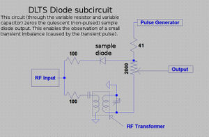
Our circuit will mix a known voltage signal with another voltage signal passing through the diode. We have created a circuit that will split the incoming signal. On one leg of our circuit the voltage signal will run through the diode. The other leg consists of a 180 degree phase shifter that will recombine with the signal coming out of the diode, thus canceling the signal and outputting a signal of 0 amplitude. In reality we cannot exactly cancel out the signal coming out of the diode, so after the phase shifter we have a variable capacitor. This capacitor allows us to very minutely shift the phase of the signal. This will allow us to fine tune the phase of the signal we are using to cancel the signal coming out of the diode. At the end of the circuit both legs are attached to a variable resistor. There are voltage drops across both legs of the circuit and the variable resistor allows us to change the amplitude of the signals to find the ideal for cancellation. By adjusting the variable resistor and capacitor an input signal measured at 248 mV resulted in a 1.6 mV output.
The original signal will input into a mixer with the signal coming out of the circuit. The signals are multiplied in the mixer and the resulting signal will be output on an oscilloscope. During steady state the output coming out of he circuit should be close to 0 so no signal will be measured. When we introduce the pulse the signal on the bottom leg of our circuit will no longer cancel the signal coming through the top wave and a signal of interest will be measured. This will result in a spike of voltage that will gradually return to zero as the electrons are kicked out of the traps in the depletion zone of the diode. We will observe a voltage transient and from that we will be able to calculate the capacitance transient we are looking for.
As stated earlier, thermal energy is what releases electrons from the traps. Electrons are released faster as the temperature increases, thus the capacitance transient is "thinner" with respect to time for higher temperatures (it takes less time for the capacitance to return to zero). To make measurements we will
consider emission rates which are what define the capacitance transient. We can define emission rate "windows", a certain rate in the capacitance transient, to measure only emission rates that we define. For each window we can take measurements at many different temperatures and we will see peaks at temperatures (because emission rate is temperature dependent) that match the window we defined. If we change the window and repeat the measurement we will see peaks at different temperatures. If we plot the width of the peaks against 1/Temperature we will observe a straight line, the length of which will be the rate window we defined. By measuring several different windows at varying temperatures we will observe a long straight line. The slope of that line is the activation energy for the trap. We will use a cryostat with liquid nitrogen to measure the diode at different temperatures.
Group 2: Zach Small and Chris Luetjen
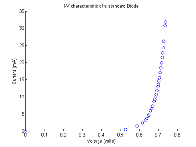
For a standard diode its characteristics depends on what material the diode is made out of and with what it has been doped with. For the 1N4004, we measured an I-V characteristic as shown in Figure 1.
This is exactly what we would expect, as Diode Incorporated; the manufacturer, gives us the characteristic graphs of these diodes 1N4004_spec_sheet. Note that in the graph, the first point after point (0, 0) is the next none zero point, meaning at the current remained at 0 until 5.2 volts across the diode.
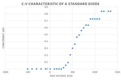
The standard diode will have a small amount of capacitance current flows across it. This capacitance is called the Junction Capacitance and is because charge is stored inside the diode and a small amount will build up. Figure 2 is C-V characteristic of the P6KE6.8A diode, of which this is the spec sheet: P6KE_spec_sheet. This data was taken using a voltage divider, shown in Figure 3
and the voltage divider equation, . f=10 Hz, Vin=20 mV (AC Voltage peak to peak), R=1 kohm, and bias Voltage=-500 mV to 1200 mV was chosen to take this data. As you can see, when reverse biased the voltage was basically zero, this is because the electrons and holes drift in the opposite direction and leave their respective n or p type region.
Carrier Dynamics
Carrier dynamics are the dynamics between the charge carriers in the semiconductor and how they interact with each other and external factors.
Depletion Region Width
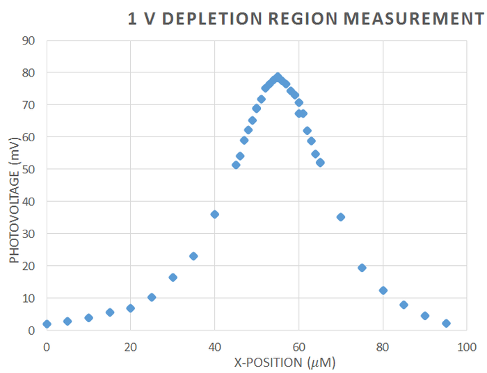
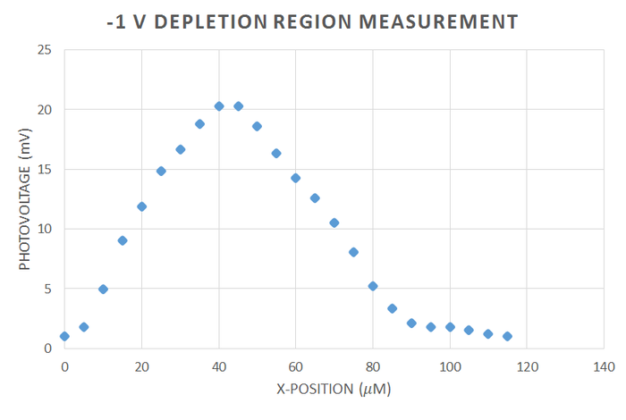
The setup shown in Figure 4 was used to measure the carrier dynamics of a laser diode. For this experiment, the GH0781JA2C diode was used, the spec sheet can be found here, GH0781JA2C_spec_sheet. We used the two lenses to expand and collimate the lens. This is important, because the microscope objective, which is focusing our beam down to a point in order to shine on the semiconductor of laser diode, is designed to be fully filled of light in order to work properly. The chopper was used to chop the light into a frequency in which other parts of the room where not emitting radiation at. This frequency was then sent to the lock-in amplifier, which amplifies the signal at the reference frequency. This helps separate our data, the voltage over the laser diode, from the noise in the rest of the room. Before using the lock-in amplifier, we experienced trouble getting readings on the multimeter, which was measuring unchopped light. To fix this, we connected our diode with a coaxial cable instead of just plain wires. This was to protect the wires, which were acting as antennas and were picking up frequencies from other electrons in the room, so the lights, refrigerators, etc. This did fix the problem, but we still received significant noise, and thus used the lock-in amplifier. We used the 7280 whose instruction Manuel can be found here: 7280_spec_sheet_and_instruction_manuel The laser diode was also reverse biased. This is because there would be no voltage or current across the laser diode, and therefore the only voltage we would read would be that from focusing our IR diode laser (The New Focus 6224 was used) at 784 nm on the laser diode. The purpose was to measure the depletion zone of the diode, which we measured at -1 V, 0 V, and 1 V. The data is shown in Figures 5, 6, and 7 and is what we expected. The depletion region increases the more negative the bias across the diode. This is because the carries, electrons and holes, are evacuating the junction at negative bias, and thus the region with no carriers becomes larger.
Although our plots display the correct trend between bias voltage and depletion region width, the scale is off. We would expect the depletion region to be roughly 1 micron, and ours measures 30-50 times that. This discrepancy is most likely due to the beam size. Our data assumes a beam size of 1 micron, which is unachievable with our system. The best beam size possible for our set up would be 1.5 microns, assuming the beam incident on our microscope objective is perfectly Gaussian. Realistically our beam size is roughly 10 microns, but a measurement should be made verify this. This measurement could be made by using the knife-edge technique, or a high resolution beam profiler or CCD camera.
Band Edge
From quantum mechanics we know that atoms exist in discrete energy levels. When N atoms are brought together, such as in a crystal, the atomic energy levels interact. This interaction causes the energy levels to split into N distinct levels. However, in crystal that contains a large number of atoms, there are so many levels, that they are indistinguishable from one another, and what is known as an energy band is created. In this band, electrons can move freely since the neighboring bands are almost touching.
When working with semiconductors, the atoms are arranged in crystalline structures, so the aforementioned energy bands are present. However, practically only two of the bands are relevant, the conduction band and the valence band. Specifically, the distance between these bands, called the band gap. In order for a semiconductor to conduct electricity, there must be electrons in the conduction band, but no electrons can exist in between the valence and conduction band, so the electrons must be excited by one “burst” of energy, such as from a photon or heat. There is also a momentum component to this transition, however, it will be omitted since we are assuming it holds no bearing in our semiconductor, which is intended to have a direct band gap.
Since a minimum energy is required to drive an electron from the valence band to the conduction band, when a photon is absorbed by a semiconductor, it can only cause this transition if it has an energy greater than or equal to the band gap. And since a photon energy is related to the wavelength by the equation, E=hc/λ, certain wavelengths can cause an electron to by driven up into the conduction band. By varying the wavelength of light incident on a semiconductor, it is possible to determine the band gap. To measure how many electrons are excited into the conduction band, a small bias voltage is applied to the semiconductor. This causes any electron in the conduction band to flow out towards the bias, creating a current which we can then measure.
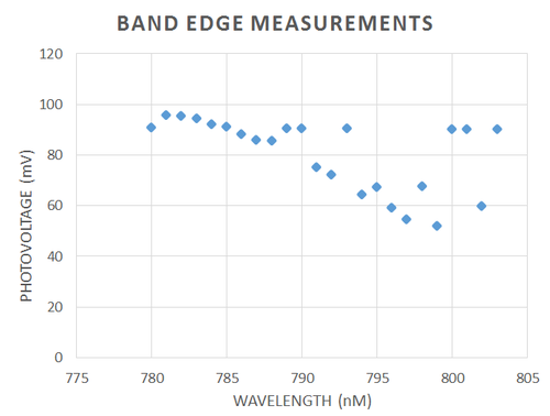
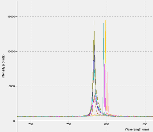
With the same setup that was used for measuring the depletion region we took band edge measurements. This was done by varying the wavelength of the tunable IR laser used in the carrier dynamics setup and directing the beam straight at the center of laser diode. The data found was conflicting and as seen in Figure 8, it varied a bit and flat lined at certain wavelengths. To fix this we added in a isolator and a wave plate that adjusted the polarity of our beam to that which the isolotor would allow to pass through. This was to remove any back reflection that may have been skewing our data. This did not fix the problem, so we took a spectrum of our laser at each wavelength, varying from 784 to 804 nm. As seen in Figure 9, the laser we were using does not tune past Figure 6 and at one point emits two wavelengths when it should be emitting one. For future band edge measurements, a different laser will have to be used.
Group 3: Derek Hallman, John McGonigle, Alex Schachtner
We performed many of the above experiments as well, beginning with measuring the IV Curve of a diode, We used a PK6E30A diode, and used a current limiting circuit in order to limit the current through the diode. We varied the voltage in to measure the resulting current out and plotted the two. We performed this measurement for forward and reverse bias to begin understanding the pn junction and depletion region. We understand the mechanisms of charge carriers and how a diode works in forward and reverse bias.
{insert charts & data here}
We then performed similar measurements while using a photodiode while injecting a photocurrent by shining a red laser pointer on the diode. We saw a similar IV curve for forward and reverse bias, however we never saw the reverse breakdown. While we saw a current effectively "turn on" similarly as the diode at around .6 volts in forward bias, though we never saw a reverse breakdown, even when taking the voltage up to 90-100 volts in reverse.
[Insert chart here too}
Now we measured the capacitance of the diode as we understand that the depletion region will act effectively as a capacitator. Charges will migrate across the region until the resulting electric field will prevent further current. The smaller the depletion region, we found the higher the effective capacitance of the diode
[]]]], circuit and data here]
Here our projects split where Alex pursued the DLTS experiments while John and Derek continued using laser diodes.
Measuring Depletion Region with a Laser
In this portion of the project we sought to utilize semiconductor properties to create light by stimulated emission of radiation by focusing a beam of near infrared signal onto a laser diode and then with piezo controls we scanned the beam across the active region in different directions and measured the depletion region.
We used an external cavity diode laser such that we could tune the wavelength of the laser and ensure that the diode was not mode hopping, such that the photons introduced into the laser diode were of constant energy. We wanted to select the most dominant mode for the greatest emission intensity. We used a wavemeter which measured the interference fringes of the HeNe beam and the beam from our laser didoe. By steering a system of mirrors we were to align the beams at two points, ensuring that they were aligned as a line along the beam path. We used a bandpass filter with Near Infrared specs to allow the beam of our laser diode to pass and interfere with the HeNe beam, while disallowing the HeNe beam to reflect back into the laser diode which would alter the dynamics of emission and skew our beam.
Our set-up was as follows: Laser Diode -> Chopper -> Up/Down mirror -> Half-Wave plate -> Isolator -> Diverging lens -> Collimating Lens -> Microscope Objective -> Laser diode.
[picture]
Our chopper singled out our beam's signal and in combination with the lock in amplifier we then began introducing our beam to the laser diode such that we could then scan the beam across the PN junction and the active region of the diode. The system of lenses were installed to adjust the spot diameter of the beam to the required length in order to fill the microscope objective properly which then projected the the signal onto the laser diode. Our goal here was to focus the beam down to .5um using Gaussian beam dynamics so we could scan the beam across the active region of the laser diode which was around 1um thick and 3-5 um across. We were also able to make more precise measurements when we used piezo controls in combination with the lock in amplifier to make our measurements.
Our data is as follows:
{Insert charts and all final data here}
Goals
Deep Level Transient Spectroscopy
The Deep Level Transient Spectroscopy was discussed in detail above by Group 1
Electronics
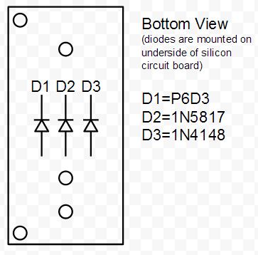
In Figure 10 is a picture of the circuit that they constructed in Figures 11 and 12 is the schematics for the circuit. We utilized this circuit to make measurements on three different diodes, a standard diode; P6KE , a Schottky Barrier Rectifier; 1N5817_1.0A , and a Fast Response diode; 1N4148. The links are to the spec sheets of said diodes. The measurements are at 1 V and 2.3 V. You will notice that the decay curve changes from a negative decay to a positive decay and this is when the sum of the offset and the pulse is greater than the threshold voltage of the diode.
Current Data
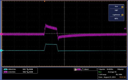
The data above shows a decay rate for what we originally thought was the decay of carriers through the diode. It turns out that with no diode, a very similar decay is observed, although more slowly. It is possible to get almost the identical curve by varying the resister in the DLTS circuit. In Figure 13 a pulse is showed with no diode. It is shallower, but for it be to what we would expect it to be, it should rise and fall sharply with the pulse. It should look almost identical to the pulse sent in, however we do get a slight decay rate. Another indicator that the above data may be measuring something other than the decay rate of carriers is the decay across the pulse. We would expect it to remain flat with the pulse, as steady current passes through the diode at that point, meaning that carriers are flowing through the diode. To check if our circuit was working, we rebuilt the total circuit shown in Figure 11 with stand alone components and attached a standard diode. We then placed this same diode into our DLTS and measured the results of each, in which we observed the same result. The stand alone setup result is shown in Figure 14 and the DLTS is shown in Figure 15. In conclusion this data may be measuring the decay rate of carriers in the diode as it does change with the diodes, but we have inconclusive evidence until the pulse passing through the system is analysed.
Cryostat
As previously mentioned by group 1, a cryostat can be used to cool the diodes down to liquid nitrogen temperatures (77 K). By cooling the diodes, the thermal energy decreases significantly, so the ability for the charge carriers to escape the traps decreases, resulting in a slower voltage decay after the pulse.
To cool the diode we used a cryostat. A cryostat is essentially a liquid nitrogen Dewar with a chamber enclosed that has a plate in thermal contact with the liquid nitrogen. A picture of the cryostat is shown in figure 16. Everything in the chamber is cooled significantly, and anything in thermal contact with the plate, is also in thermal contact with the liquid nitrogen. We mounted the diodes in the cryostat by soldering them to a circuit board, and then affixing the circuit board to the thermal plate in the cryostat with the diodes all in contact with it. A schematic of this circuit board can be seen in figure 17. The diodes were then wired into a port so they could be connected to the rest of the circuit. The PIN layout of the port is shown in Figure 18.
The cryostat was never actually tested due to issues with the DLTS setup. And a new port should be made to connect the diodes in the cryostat to the external circuit, since the current port has brass pins on the outside, which solder does not stick to very well. That said, the current port will work fine if a hook or clip is attached to the each individual pin. The easiest method would be to use a BNC port.
Here is the Power Point Presentation of our final presentation. It includes a few pictures of our setup and the diodes and may prove useful if there are any questions in the actual physical setup of the experiment. 
Group 3 (Alex Schachtner): DLTS Circuit Modifications and Overall Improvements
What we are seeking to measure in this experiment is the current output resulting from the loaded traps (lattice impurities) in the depletion region of a diode being emptied of charges as the loading pulse is shut off. Building on the work of the previous group, my goal was to see this current and report results based on varying both temperature as well as the semiconducting material being tested.
Phase 1: DLTS Circuit Modifications
The first major task was to ensure the DLTS circuit was functioning properly after recognizing the difficulties of the previous group. I isolated the DLTS circuit and tuned the variable resistor and capacitor such that there was no phase difference in the two legs of the original DLTS circuit pictured above. Once this was complete, I set about investigating the previous group's results and attempting to acquire a DLTS signal. Inital tests were done on the same 3 diodes used by the previous group, and results can be seen here:
Test program conditions: Function generator has a 30 MHz signal, +20 mV peak-to-peak amplitude, and a +1 V DC offset. The loading pulse (on the old pulse generator) has a +2.0V amplitude and 1ms length.
The suspected recombination current outputs from each respective diode appeared to be on the order of 0.02 - 2 mA. The above data was convincing enough to move onto the next major modification - attempting to amplify the output signal and investigate the nature of the traps in the depletion region of the P6KE30A diode.
Before that was done, a path length modification was installed. This amounted to mounting the diode on an elongated stretch of wire (approximately 240mm total increase) and balancing that path length on the other side of the circuit with an equal length of wire. This was done so that a very rudimentary temperature test could be done - dunking the entire diode in liquid nitrogen.
Phase 2: External Improvements
A new pulse generator, TTL switch, and 10db RF amplifier were tested and installed after the DLTS circuit to achieve two goals. Firstly, the new pulse generator would send two pulses: one to load charge traps in the diode by momentarily putting the diode into forward bias (as the previous setup was designed to do). Secondly, another pulse would be sent to the TTL switch and amplifier. This delayed pulse would be triggered to turn the amplifier on immediately after the diode-loading pulse was shut off. This would effectively amplify the output signal from the diode in the region of interest and allow the experimenter to see the output recombination current in greater detail. A schematic of the improvements can be seen below:
and a few images the updated setup:
- New DLTS Circuit Isolated.jpg
TTL Switch and Amplifier
A tunable phase shifter and 1 MHz high-pass filter will need to be installed in the future. At the end of my time on the project a working phase shifter could not be located, but a 1 MHz high pass filter has been created and can be found on the optics table near the experiment for later installation. The goal of the filter is simple noise reduction. The goal of the phase shifter is to ensure we are amplifying the output of the "decaying capacitor" that is the depletion region.
Phase 3: DLTS Data 2.0
After all the external improvements were implemented and determined to be working as designed, I resumed looking for the recombination current. Initial tests on the P6KE30A diode showed this output signal:
Experimental conditions: 30 MHz RF signal, +20 mV peak-to-peak amplitude, +1 V DC offset. Loading pulse: +1.5 V for 20 us. NOTE: The pulse generator output amplitude should be approximately +3.70 V. The signal is split many ways, so this will yield approximately +1.5 V (which is setup to be read directly from the oscilloscope).
