Physics of Semiconductor Devices
Contents
- 1 Physics of Semiconductors Project
- 2 Deep-Level Transient Spectroscopy
- 3 Capacitance and Depletion Region Measurements
Physics of Semiconductors Project
Physics of Semiconductors Web Page
The goal of this project is to characterize different semiconductors using various techniques.
Deep-Level Transient Spectroscopy
One goal of the Physics of Semiconductor Devices project is to measure captured carriers within the band-gap of a semiconductor. If a carrier (a hole or electron) is captured and then released in the band, the capture center is called a trap. These traps arise from defects or impurities in the material. One technique for measuring these traps is through Deep Level Transient Spectroscopy, or DLTS. This technique essentially measures the change in capacitance of the semiconductor.
We are using a high‐frequency capacitance transient thermal scanning method to observe traps in the depletion region of our diode. The capacitance transients can give us information about trap concentration, activation energy and electron‐ and hole‐capture cross sections for each trap. These properties are of interest to industry.
Our circuit is built on a copper plating encased in a steel container. This is to reduce stray capacitance and noise from the high frequency signal (our signal is 30 MHz.) The plating provides a large common ground that will reduce these effects. In the future copper tape soldered near the input and output ports will further reduce these unwanted effects. Our diode is a schottky diode, which is used for it's fast switching properties.
The premise behind DLTS is to use a short pulse to momentarily forward bias a diode that is in a steady state of reverse bias. This short pulse will inject carriers (in our case electrons) into the depletion zone of our semiconductor (putting the diode in forward bias will shrink the depletion zone and allow electrons to enter). This will change the capacitance of the diode. Semiconductors are characterized by their unique conductive behavior. A semiconductor has a fermi energy that lies inside a band gap in electron energy levels. This band gap is small in a semiconductor however, allowing electrons to cross the band gap at relatively low temperatures (as compared to an insulator.) The rate at witch electrons are emitted from a trap is what will characterize the capacitance transient. The emission rate is proportional to a boltzman factor and depends exponentially on the energy difference between the trap level and the conduction band. In essence we will inject the depletion zone with electrons, thus raising the capacitance of the diode. Some electrons will become trapped. Thermal energy will eventually kick these electrons out of the traps and back into the charged portion of the semiconductor. The capacitance will spike when the electrons are introduced and slowly return to normal as the electrons are kicked out the traps. If the traps were not present we would expect a linear return to steady state capacitance.
Our circuit will mix a known voltage signal with another voltage signal passing through the diode. We have created a circuit that will split the incoming signal. On one leg of our circuit the voltage signal will run through the diode. The other leg consists of a 180 degree phase shifter that will recombine with the signal coming out of the diode, thus canceling the signal and outputting a signal of 0 amplitude. In reality we cannot exactly cancel out the signal coming out of the diode, so after the phase shifter we have a variable capacitor. This capacitor allows us to very minutely shift the phase of the signal. This will allow us to fine tune the phase of the signal we are using to cancel the signal coming out of the diode. At the end of the circuit both legs are attached to a variable resistor. There are voltage drops across both legs of the circuit and the variable resistor allows us to change the amplitude of the signals to find the ideal for cancellation. By adjusting the variable resistor and capacitor an input signal measured at 248 mV resulted in a 1.6 mV output.
The original signal will input into a mixer with the signal coming out of the circuit. The signals are multiplied in the mixer and the resulting signal will be output on an oscilloscope. During steady state the output coming out of he circuit should be close to 0 so no signal will be measured. When we introduce the pulse the signal on the bottom leg of our circuit will no longer cancel the signal coming through the top wave and a signal of interest will be measured. This will result in a spike of voltage that will gradually return to zero as the electrons are kicked out of the traps in the depletion zone of the diode. We will observe a voltage transient and from that we will be able to calculate the capacitance transient we are looking for.
As stated earlier, thermal energy is what releases electrons from the traps. Electrons are released faster as the temperature increases, thus the capacitance transient is "thinner" with respect to time for higher temperatures (it takes less time for the capacitance to return to zero). To make measurements we will
consider emission rates which are what define the capacitance transient. We can define emission rate "windows", a certain rate in the capacitance transient, to measure only emission rates that we define. For each window we can take measurements at many different temperatures and we will see peaks at temperatures (because emission rate is temperature dependent) that match the window we defined. If we change the window and repeat the measurement we will see peaks at different temperatures. If we plot the width of the peaks against 1/Temperature we will observe a straight line, the length of which will be the rate window we defined. By measuring several different windows at varying temperatures we will observe a long straight line. The slope of that line is the activation energy for the trap. We will use a cryostat with liquid nitrogen to measure the diode at different temperatures.
Capacitance and Depletion Region Measurements

For a standard diode its characteristics depends on what material the diode is made out of and with what it has been doped with. For the 1N4004, we measured an I-V characteristic as shown in Figure 1.
This is exactly what we would expect, as Diode Incorporated; the manufacturer, gives us the characteristic graphs of these diodes 1N4004_spec_sheet. Note that in the graph, the first point after point (0, 0) is the next none zero point, meaning at the current remained at 0 until 5.2 volts across the diode.
The standard diode will have a small amount of capacitance current flows across it. This capacitance is called the Junction Capacitance and is because charge is stored inside the diode and a small amount will build up. Figure 2 is C-V characteristic of the P6KE6.8A diode, of which this is the spec sheet: P6KE_spec_sheet. This data was taken using a voltage divider, shown in Figure 3

and the voltage divider equation, . f=10 Hz, Vin=20 mV (AC Voltage peak to peak), R=1 kohm, and bias Voltage=-500 mV to 1200 mV was chosen to take this data. As you can see, when reverse biased the voltage was basically zero, this is because the electrons and holes drift in the opposite direction and leave their respective n or p type region.


Carrier Dynamics
Carrier dynamics are the dynamics between the charge carriers in the semiconductor and how they interact with each other and external factors.
Depletion Region Width
The setup shown in Figure 4 was used to measure the carrier dynamics of a laser diode. For this experiment, the GH0781JA2C diode was used, the spec sheet can be found here, GH0781JA2C_spec_sheet. We used the two lenses to expand and collimate the lens. This is important, because the microscope objective, which is focusing our beam down to a point in order to shine on the semiconductor of laser diode, is designed to be fully filled of light in order to work properly. The chopper was used to chop the light into a frequency in which other parts of the room where not emitting radiation at. This frequency was then sent to the lock-in amplifier, which amplifies the signal at the reference frequency. This helps separate our data, the voltage over the laser diode, from the noise in the rest of the room. Before using the lock-in amplifier, we experienced trouble getting readings on the multimeter, which was measuring unchopped light. To fix this, we connected our diode with a coaxial cable instead of just plain wires. This was to protect the wires, which were acting as antennas and were picking up frequencies from other electrons in the room, so the lights, refrigerators, etc. This did fix the problem, but we still received significant noise, and thus used the lock-in amplifier. We used the 7280 whose instruction Manuel can be found here: 7280_spec_sheet_and_instruction_manuel The laser diode was also reverse biased. This is because there would be no voltage or current across the laser diode, and therefore the only voltage we would read would be that from focusing our IR diode laser (The New Focus 6224 was used) at 784 nm on the laser diode. The purpose was to measure the depletion zone of the diode, which we measured at -1 V, 0 V, and 1 V. The data is shown in Figures 5, 6, and 7 and is what we expected. The depletion region increases the more negative the bias across the diode. This is because the carries, electrons and holes, are evacuating the junction at negative bias, and thus the region with no carriers becomes larger.
Although our plots display the correct trend between bias voltage and depletion region width, the scale is off. We would expect the depletion region to be roughly 1 micron, and ours measures 30-50 times that. This discrepancy is most likely due to the beam size. Our data assumes a beam size of 1 micron, which is unachievable with our system. The best beam size possible for our set up would be 1.5 microns, assuming the beam incident on our microscope objective is perfectly Gaussian. Realistically our beam size is roughly 10 microns, but a measurement should be made verify this. This measurement could be made by using the knife-edge technique, or a high resolution beam profiler or CCD camera.


Band Edge Measurements
From quantum mechanics we know that atoms exist in discrete energy levels. When N atoms are brought together, such as in a crystal, the atomic energy levels interact. This interaction causes the energy levels to split into N distinct levels. However, in crystal that contains a large number of atoms, there are so many levels, that they are indistinguishable from one another, and what is known as an energy band is created. In this band, electrons can move freely since the neighboring bands are almost touching.
When working with semiconductors, the atoms are arranged in crystalline structures, so the aforementioned energy bands are present. However, practically only two of the bands are relevant, the conduction band and the valence band. Specifically, the distance between these bands, called the band gap. In order for a semiconductor to conduct electricity, there must be electrons in the conduction band, but no electrons can exist in between the valence and conduction band, so the electrons must be excited by one “burst” of energy, such as from a photon or heat. There is also a momentum component to this transition, however, it will be omitted since we are assuming it holds no bearing in our semiconductor, which is intended to have a direct band gap.
Since a minimum energy is required to drive an electron from the valence band to the conduction band, when a photon is absorbed by a semiconductor, it can only cause this transition if it has an energy greater than or equal to the band gap. And since a photon energy is related to the wavelength by the equation, E=hc/λ, certain wavelengths can cause an electron to by driven up into the conduction band. By varying the wavelength of light incident on a semiconductor, it is possible to determine the band gap. To measure how many electrons are excited into the conduction band, a small bias voltage is applied to the semiconductor. This causes any electron in the conduction band to flow out towards the bias, creating a current which we can then measure.
With the same setup that was used for measuring the depletion region we took band edge measurements. This was done by varying the wavelength of the tunable IR laser used in the carrier dynamics setup and directing the beam straight at the center of laser diode. The data found was conflicting and as seen in Figure 8, it varied a bit and flat lined at certain wavelengths. To fix this we added in a isolator and a wave plate that adjusted the polarity of our beam to that which the isolotor would allow to pass through. This was to remove any back reflection that may have been skewing our data. This did not fix the problem, so we took a spectrum of our laser at each wavelength, varying from 784 to 804 nm. As seen in Figure 9, the laser we were using does not tune past Figure 6 and at one point emits two wavelengths when it should be emitting one. For future band edge measurements, a different laser will have to be used.


Deep Level Transient Spectroscopy
Deep Level Transient Spectroscopy was discussed in detail above.
Electronics


In Figure 10 is a picture of the circuit that they constructed in Figures 11 and 12 is the schematics for the circuit. We utilized this circuit to make measurements on three different diodes, a standard diode; P6KE , a Schottky Barrier Rectifier; 1N5817_1.0A , and a Fast Response diode; 1N4148. The links are to the spec sheets of said diodes. The measurements are at 1 V and 2.3 V. You will notice that the decay curve changes from a negative decay to a positive decay and this is when the sum of the offset and the pulse is greater than the threshold voltage of the diode.
Current Data
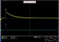
1N4148-1V Pulse
1N4148-2.3V Pulse
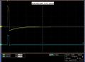
1N517-1V Pulse
1N517-2.3 Pulse

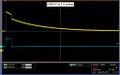
P6KE-1V Pulse
P6KE-2.3V Pulse


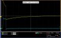
The data above shows a decay rate for what we originally thought was the decay of carriers through the diode. It turns out that with no diode, a very similar decay is observed, although more slowly. It is possible to get almost the identical curve by varying the resister in the DLTS circuit. In Figure 13 a pulse is showed with no diode. It is shallower, but for it be to what we would expect it to be, it should rise and fall sharply with the pulse. It should look almost identical to the pulse sent in, however we do get a slight decay rate. Another indicator that the above data may be measuring something other than the decay rate of carriers is the decay across the pulse. We would expect it to remain flat with the pulse, as steady current passes through the diode at that point, meaning that carriers are flowing through the diode. To check if our circuit was working, we rebuilt the total circuit shown in Figure 11 with stand alone components and attached a standard diode. We then placed this same diode into our DLTS and measured the results of each, in which we observed the same result. The stand alone setup result is shown in Figure 14 and the DLTS is shown in Figure 15. In conclusion this data may be measuring the decay rate of carriers in the diode as it does change with the diodes, but we have inconclusive evidence until the pulse passing through the system is analysed.


Cryostat

As previously mentioned by group 1, a cryostat can be used to cool the diodes down to liquid nitrogen temperatures (77 K). By cooling the diodes, the thermal energy decreases significantly, so the ability for the charge carriers to escape the traps decreases, resulting in a slower voltage decay after the pulse.
To cool the diode we used a cryostat. A cryostat is essentially a liquid nitrogen Dewar with a chamber enclosed that has a plate in thermal contact with the liquid nitrogen. A picture of the cryostat is shown in figure 16. Everything in the chamber is cooled significantly, and anything in thermal contact with the plate, is also in thermal contact with the liquid nitrogen. We mounted the diodes in the cryostat by soldering them to a circuit board, and then affixing the circuit board to the thermal plate in the cryostat with the diodes all in contact with it. A schematic of this circuit board can be seen in figure 17. The diodes were then wired into a port so they could be connected to the rest of the circuit. The PIN layout of the port is shown in Figure 18.
The cryostat was never actually tested due to issues with the DLTS setup. And a new port should be made to connect the diodes in the cryostat to the external circuit, since the current port has brass pins on the outside, which solder does not stick to very well. That said, the current port will work fine if a hook or clip is attached to the each individual pin. The easiest method would be to use a BNC port.
Here is the Power Point Presentation of our final presentation. It includes a few pictures of our setup and the diodes and may prove useful if there are any questions in the actual physical setup of the experiment. 
Diode Capacitance Revisited
We performed many of the above experiments as well, beginning with measuring the IV Curve of a diode, We used a PK6E30A diode, and used a current limiting circuit in order to limit the current through the diode. We varied the voltage in to measure the resulting current out and plotted the two. We performed this measurement for forward and reverse bias to begin understanding the pn junction and depletion region. We understand the mechanisms of charge carriers and how a diode works in forward and reverse bias.


We then performed similar measurements while using a photodiode while injecting a photocurrent by shining a red laser pointer on the diode. We saw a similar IV curve for forward and reverse bias, however we never saw the reverse breakdown. While we saw a current effectively "turn on" similarly as the diode at around .6 volts in forward bias, though we never saw a reverse breakdown, even when taking the voltage up to 90-100 volts in reverse.


Now we measured the capacitance of the diode as we understand that the depletion region will act effectively as a capacitator. Charges will migrate across the region until the resulting electric field will prevent further current. The smaller the depletion region, we found the higher the effective capacitance of the diode
Measuring Depletion Region with a Laser
In this portion of the project we sought to utilize semiconductor properties to create light by stimulated emission of radiation by focusing a beam of near infrared signal onto a laser diode and then with piezo controls we scanned the beam across the active region in different directions and measured the depletion region.
We used an external cavity diode laser such that we could tune the wavelength of the laser and ensure that the diode was not mode hopping, such that the photons introduced into the laser diode were of constant energy. We wanted to select the most dominant mode for the greatest emission intensity. We used a wavemeter which measured the interference fringes of the HeNe beam and the beam from our laser diode. By steering a system of mirrors we were to align the beams at two points, ensuring that they were aligned as a line along the beam path. We used a bandpass filter with Near Infrared specs to allow the beam of our laser diode to pass and interfere with the HeNe beam, while disallowing the HeNe beam to reflect back into the laser diode which would alter the dynamics of emission and skew our beam.
Our set-up was as follows: Laser Diode -> Chopper -> Up/Down mirror -> Half-Wave plate -> Isolator -> Diverging lens -> Collimating Lens -> Microscope Objective -> Laser diode.
[picture]
Our chopper singled out our beam's signal and in combination with the lock in amplifier we then began introducing our beam to the laser diode such that we could then scan the beam across the PN junction and the active region of the diode. The system of lenses were installed to adjust the spot diameter of the beam to the required length in order to fill the microscope objective properly which then projected the the signal onto the laser diode. Our goal here was to focus the beam down to .5um using Gaussian beam dynamics so we could scan the beam across the active region of the laser diode which was around 1um thick and 3-5 um across. We were also able to make more precise measurements when we used piezo controls in combination with the lock in amplifier to make our measurements.
Our data is as follows:


Two Photon Absorption
This leg of the experiment was Introducing a laser to the laser diode detector of wavelength one half of the wavelength that would normally cause single photon absorption. One photon promotes an electron to an imaginary state, second photon promotes energy to excited state, where each photon is roughly equal to half the energy of a photon that would excite an electron via one photon absorption. This is a Non-linear process (weak compared to OPA at low intensity, dominates at high intensity)
My experimental set-up is as follows:
I used an Erbium Doped Fiber Laser as a gain medium, pumped by a 980 nm laser to emit 1550 nm radiation. This radiation is roughly twice the wavelength of the photons that we used to stimulate single photon absorption, which made it suitable for two photon absorption. We used beam expansion similarly to single photon absorption, however we needed different lenses as the beam width from the free-space coupled EDFL was smaller than the External Cavity Diode Laser, and we wished to ensure the back aperture of the microscope objective was filled such that our calculations on beam waist would hold. We used a chopper for lock-in amplification to chop the beam so the Lock-In Amplifier could use the reference to eliminate noise, and we could really hone in on our signal.


My procedure is as follows:
I found that operating the pump laser at .500 amps that I could get an optical power of 17.92 mW, significantly greater than using an ECDL. Aligned two beams (1550, and ~640) using a flip mirror, and several irises so that I may roughly alight the focused beam from the microscope objective with the active region on the detector diode. Using the coarse controls on the translation stage, and finer adjustments using the piezoelectric displacement, I attempted to maximize photocurrent using single photon absorption, in order to roughly align the detector diode with microscope lens. It should be noted that the working distance with the visible light, and the IR light will be different, so further alignment with the IR beam is necessary. Thus I then reconfigured beam expansion for IR light, and worked to confirm that the 1550 beam was stimulating electrons via two photon absorption; I then worked to maximize the read-out on the lock-in amplifier. Confirming that two photon absorption is taking place, I begin scanning beam across diode surface.
Thus I began scanning beam across the surface of the laser diode detector, to understand two photon absorption as a function of displacement across the diode face I found that it was very difficult to find the active region of the diode using both two photon absorption and lock-in detection, and at the intensity I was working at only generated a signal in the order of magnitude of MicroVolts. To analyze the signal generated by scanning the beam across the diode, I took a 10x10 matrix, taking data in Microvolts at points that were a stepsize of about a micron (uM) apart. I then entered these matrices into MATLAB and wrote a function which both would interpolate these points and create various contour and surface plots of the matrices. This allows us a visual representation of voltage generated by Two-Photon Absorption of 1550nm IR radiation.


After collecting such poor data even while the lock-in amp seemed to be showing such clear gaussian trends upon displacement from what I believed was the active region, I resorted to reconfigure the translation stage, and used the coarse knobs to "hunt around" for the signal from introducing the beam to the active region. This was a very sensitive process as two-photon absorption requires high intensity. In doing so I found much higher voltages through the Lock-in amp than I had seen before - i.e. 10uV to about 30uV. I then collected the best data and what seems to be a clear indication of scanning the beam across the active region.
The best data is subject for further study, and possible publication. It is as follows:


The data I have collected could have a variety of implications, and could provide the basis of future publications: - Temperature dependence - Increased penetration of IR photons into semiconductor sample - Different behavior across the PN junction from OPA
We wished to improve upon measurements made and to make strides to better understand the nature of Laserdiodes and the physics of the semiconductors that comprise them. We saw in previous measurements how temperature could effect the behavior of charges in the laser diode. Our first goal was to introduce some temperature control to the design, so we replaced the diode that we have reverse biased for use as the detector. We introduced the LDM21 as a more advanced diode mount with integrated temperature control, we also replaced the diode in the mount from whichever we were using before (no exact specs, but we knew it had a bandgap ~785nm) with the thorlabs L785P6 diode which we then had the exact specifications for. We needed to correctly arrange the diode in the mount, and solder a D9 Connector so that we may monitor the signal out of the diode. We opted to use 2 BNC Coaxial cables as we used one of the tips of the cable as a ground, which grounded the diode, and the Cathode of the diode as we were operating in reverse bias / Cathode grounding, and the other BNC went to the anode so we could measure the signal. We monitored our signal using a LockIn-Amplifier and used Math Functions to monitor our signal as a potential difference (Anode - Ground / Cathode). Attempting to re-establish our signal we could not find evidence of two photon absorption using the 1550nm ~20mW laser we had used before while searching over the diode, and using OPA (~634nm ~2mw) to roughly align the pn junction with the microscope objective.
We then made some customizations to the Erbium Doped Fiber Laser that we had been using. We opted to use the pump of the EDFL to excite electrons as it both had a higher wavelength, and a much greater intensity. We created fiber connection terminals inside of the fiber laser so that we could still use the pump laser to excite the Erbium gain medium for using the fiber laser at 1550nm, or to an exterior port where we used the 980nm laser directly out. We noticed that when using the 980 wavelength, at the same laser current settings that we had a ~23dB gain from the 1550nm. We maxed out the powermeter at very low laser currents, and didn't continue to compare the emission from the 980 and the 1550 as the difference was substantial enough to clearly witness two photon absorption. Once roughly aligning the diode (OPA ~634nm) we could easily establish a signal from the 980nm laser where we were operating the laser at around .45 Amps that had a related power of over 300mw. We used the familiar piezo controls described in previous phases of the experiment to orient the diode in the 980 beam and maximized our signal at over 1mV, significantly higher than the peak potential we had seen using the 1550nm wavelength and the older (mystery) diode which had a maximum around 30uV.
Thus we took data and tried to refine ideas of how charge carriers operated within the junction and what we knew of two-photon absorption and band structure. We saw in our data that we had a much more defined PN junction that previous measurements suggest and we had definitely increased our resolution of the junction and the mapping of two-photon absorption within the junction.
Here is our first data:


We see this strange double peak where we may have expected the laser to provide us with a signal that would indicate a gaussian distribution of absorption across the junction. Next we turn down the intensity of the laser and repeat the same measurements with more attention to the behavior across the junction.
Here is our final data from the term:


Interestingly we see this double peak while scanning the laser across the PN junction, namely the active region of the intrinsically doped region of the laser diode. We understand that in a PIN diode configuration, also described as a heterojunction - we see that the intrinsic region has the lowest bandgap energy which corresponds to the refractive index. In this way the active region of the laser diode acts as a waveguide, and this is the face of the laser that emits radiation. We consider our double peak somewhat as a result of the intensity of the laser. We know that as a non-linear optical phenomena, two photon absorption is very difficult to witness at low intensity but dominates at high intensity. We understand that perhaps when the beam is strictly on the active region, we are depleting the entire region of charge carriers and when we scan in nearby areas (such as overlapping a junction) there are more nearby available charge carriers to conduct. Thus this is the next phase of the experiment is to document the electric potential difference signal of the heterojunction by varying the intensity of the laser and documenting the behavior of this double peak. Our future measurements include continuing two-photon absorption, band edge measurements, exciton structure, etc...
IV and CV Curve Measurements Revisited
Like other groups, we began by exploring the 'activation voltage' of a 365-1085-ND photodiode- that is, the voltage required in order for the p-n junction to conduct.
In order to do so, we applied varying bias voltages across the photodiode and calculated the current across a resistor in the following manner:

The results came out quite good.
The following is a graph displaying the IV Curve of the Diode between 0-.8 V. Notice that we tested the IV Curve in three different lighting environments, in the dark with the lab lights off, in the ambient light of the lab, and underneath an intense flashlight.

The following is a graph displaying the IV Curve of the Diode between -40- 1 V. Notice the considerable difference in stimulated current between the flashlight and ambient light environments. This is caused by the intense light of the flashlight producing a reverse-biased current in the photodiode. This behavior is expected.

The measurements regarding the capacitance of a photodiode requires a slightly higher degree of sophistication. The following is a diagram of our experimental set up:

Notice that we treat the photodiode as a capacitor in part of a voltage divider change. We take it's impedance to be simply the capacitor reactance. Thus, the calculation to solve for the capacitance is as follows:

The following is a graph of our results:

The measurements did not turn out very well. Notice that between 0 and .3V, we found a negative capacitance, which is physically impossible. That said, the waveform of the results is good- capacitance increases quite quickly as a positive voltage is applied. We suspect there was an underlying problem in our methodology, but were unable to determine the root cause and, in order to complete our term goals, decided to move on rather than troubleshoot further.
Band Edge Measurement
We then began work on the principle focus of our research- the band edge measurement. A distinct type of semiconductor device is the laser diode. By applying a laser of sufficient wavelength to the p-n junction of the laser diode, we are able to produce a non-trivial voltage. This is, in essence, the photovoltaic effect. We sought to measure the wavelength (and therefore energy) necessary to stimulate this effect. The following diagram shows our initial experimental setup.

We were conducting these experiments on a ML925B45F Laser Diode which should have a band gap of about 1550nm. In theory, the laser diode will produce a photocurrent and thus a photovoltage only if the light shined on the diode is of a wavelength that is less then 1550nm (higher energy light then 1550nm). Thus, our data taking procedure was relatively straight-forward: we measured the photovoltage output on an oscilloscope for a range of wavelengths that scanned through 1550nm. As we scanned though wavelengths we would make sure to maintain a constant power by adjusting the current used in our laser source. We predicted these measurements would yield no photovoltage at wavelengths greater then 1500nm and some photovoltage at wavelengths less then 1550nm.
We preformed the experiment several times using our initial experimental set (above) and did not receive the predicted results. Our measurements yielded a constant photovoltage independent of wavelength. Just to confirm that our laser diode was functioning correctly, we ran current through our diode to produce a laser. We wavelength of this light to be about 1552nm. So why were we not seeing any photovoltage changes as we scanned from 1570nm to 1715nm? Well the answer (thanks to Bryan) is that our diode is too hot. Bellow is a diagram that demonstrates the problem and a way to fix it.

These are some rough (but accurate enough) calculations of laser energy and thermal energy. Laser energy and thermal energy were determined with E=h*c/λ and E≈kB*T respectively. The lowest energy of light we could produce has energy 0.787 eV (1574nm) and the energy from room temperature (293k) is 0.0252 eV. The sum of these two energies is higher then the band gap! At any wavelength that we can produce with our laser, there should always be photovoltage, which is what we observed. The solution is to cool down our experiment so that we have the ability to scan through the band gap energy using our tune-able laser. Below is our new set up that is currently under construction.

We will be using a Cryostat to cool the laser diode to a sufficiently low temperature so the band gap measurement can be made. The avaliable cryostat in the lab needed two alterations so that it is compatible with our experiment. First, we needed a "cold finger" for the laser diode. A "cold finger" is a highly heat conductive piece of metal that allows good thermal connection between the cryostat and the diode. Below (first photo) is a photo of our laser diode mounted in the crystat with our newly machined cold finger. We machined this at the university's machine shop out of scrap piece of copper. The critical part of the cryostat's operation involves the need for a vacuum inside the machine. We needed a way to run a fiber optic into the cryostat without compromising the vacuum. Again, we visited the machine shop and consulted with the experts there to construct such a device. The second and third photo below show this device.


Next term we will reassemble the cryostat, make the necessary electrical connections, and take band gap measurements. I have high expectations for these measurements and expect we finally have a sound experimental set up. Once we have completed the band gap measurements we will then research excitons and attempt to observe them by conducting extremely precise photovoltage measurements.