Difference between revisions of "Physics of Semiconductor Devices"
| Line 84: | Line 84: | ||
[[File:-1Vdepltion.png]] Figure 7 | [[File:-1Vdepltion.png]] Figure 7 | ||
| − | + | With the same setup we took band edge measurements. (Insert Theory) This was done by varying the wavelength of the tunable IR laser used in the carrier dynamics setup and directing the beam straight at the center of laser diode. The data found was conflicting and as seen in Figure 8, it varied a bit and flat lined at certian wavelengths. To fix this we added in a | |
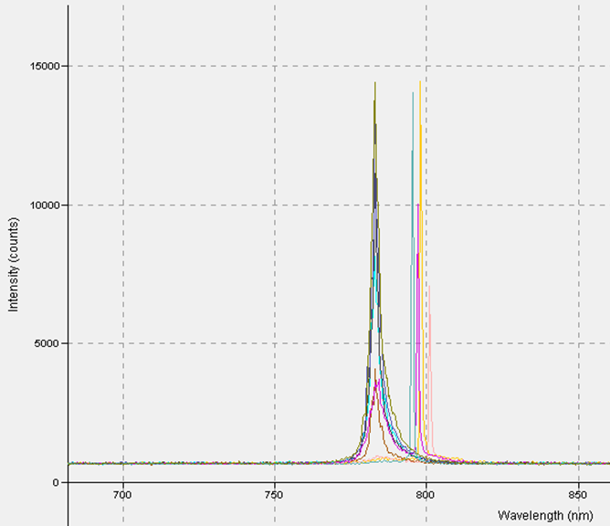
| + | isolator and a wave plate that adjusted the polarity of our beam to that which the isolotor would allow to pass through. This was to remove any back reflection that may have been skewing our data. This did not fix the problem, so we took a spectrum of our laser at each wavelength, varying from 784 to 804 nm. As seen in Figure 9, the laser we were using does not tune past Figure 6 and at one point emits two wavelengths when it should be emitting one. For future band edge measurements, a different laser will have to be used. | ||
| − | [[File: | + | [[File:Band Edge Measurements.png]] Figure 8 |
| − | [[File: | + | [[File:laser spectrum.png]] Figure 9 |
| − | |||
| − | |||
Revision as of 13:46, 24 August 2014
One goal of the Physics of Semiconductor Devices project is to measure captured carriers within the band-gap of a semiconductor. If a carrier (a hole or electron) is captured and then released in the band, the capture center is called a trap. These traps arise from defects or impurities in the material. One technique for measuring these traps is through Deep Level Transient Spectroscopy, or DLTS. This technique essentially measures the change in capacitance of the semiconductor.
We are using a high‐frequency capacitance transient thermal scanning method to observe traps in the depletion region of our diode. The capacitance transients can give us information about trap concentration, activation energy and electron‐ and hole‐capture cross sections for each trap. These properties are of interest to industry.
Our circuit is built on a copper plating encased in a steel container. This is to reduce stray capacitance and noise from the high frequency signal (our signal is 30 MHz.) The plating provides a large common ground that will reduce these effects. In the future copper tape soldered near the input and output ports will further reduce these unwanted effects. Our diode is a schottky diode, which is used for it's fast switching properties.
The premise behind DLTS is to use a short pulse to momentarily forward bias a diode that is in a steady state of reverse bias. This short pulse will inject carriers (in our case electrons) into the depletion zone of our semiconductor (putting the diode in forward bias will shrink the depletion zone and allow electrons to enter). This will change the capacitance of the diode. Semiconductors are characterized by their unique conductive behavior. A semiconductor has a fermi energy that lies inside a band gap in electron energy levels. This band gap is small in a semiconductor however, allowing electrons to cross the band gap at relatively low temperatures (as compared to an insulator.) The rate at witch electrons are emitted from a trap is what will characterize the capacitance transient. The emission rate is proportional to a boltzman factor and depends exponentially on the energy difference between the trap level and the conduction band. In essence we will inject the depletion zone with electrons, thus raising the capacitance of the diode. Some electrons will become trapped. Thermal energy will eventually kick these electrons out of the traps and back into the charged portion of the semiconductor. The capacitance will spike when the electrons are introduced and slowly return to normal as the electrons are kicked out the traps. If the traps were not present we would expect a linear return to steady state capacitance.
Our circuit will mix a known voltage signal with another voltage signal passing through the diode. We have created a circuit that will split the incoming signal. On one leg of our circuit the voltage signal will run through the diode. The other leg consists of a 180 degree phase shifter that will recombine with the signal coming out of the diode, thus canceling the signal and outputting a signal of 0 amplitude. In reality we cannot exactly cancel out the signal coming out of the diode, so after the phase shifter we have a variable capacitor. This capacitor allows us to very minutely shift the phase of the signal. This will allow us to fine tune the phase of the signal we are using to cancel the signal coming out of the diode. At the end of the circuit both legs are attached to a variable resistor. There are voltage drops across both legs of the circuit and the variable resistor allows us to change the amplitude of the signals to find the ideal for cancellation. By adjusting the variable resistor and capacitor an input signal measured at 248 mV resulted in a 1.6 mV output.
The original signal will input into a mixer with the signal coming out of the circuit. The signals are multiplied in the mixer and the resulting signal will be output on an oscilloscope. During steady state the output coming out of he circuit should be close to 0 so no signal will be measured. When we introduce the pulse the signal on the bottom leg of our circuit will no longer cancel the signal coming through the top wave and a signal of interest will be measured. This will result in a spike of voltage that will gradually return to zero as the electrons are kicked out of the traps in the depletion zone of the diode. We will observe a voltage transient and from that we will be able to calculate the capacitance transient we are looking for.
As stated earlier, thermal energy is what releases electrons from the traps. Electrons are released faster as the temperature increases, thus the capacitance transient is "thinner" with respect to time for higher temperatures (it takes less time for the capacitance to return to zero). To make measurements we will
consider emission rates which are what define the capacitance transient. We can define emission rate "windows", a certain rate in the capacitance transient, to measure only emission rates that we define. For each window we can take measurements at many different temperatures and we will see peaks at temperatures (because emission rate is temperature dependent) that match the window we defined. If we change the window and repeat the measurement we will see peaks at different temperatures. If we plot the width of the peaks against 1/Temperature we will observe a straight line, the length of which will be the rate window we defined. By measuring several different windows at varying temperatures we will observe a long straight line. The slope of that line is the activation energy for the trap. We will use a cryostat with liquid nitrogen to measure the diode at different temperatures.
Group 2: Zach Small and Chris Luetjen
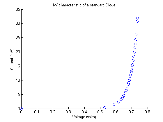
For a standard diode its characteristics depends on what material the diode is made out of and with what it has been doped with. For the 1N4004, we measured an I-V characteristic as shown in Figure 1.
This is exactly what we would expect, as Diode Incorporated; the manufacturer, gives us the characteristic graphs of these diodes 1N4004_spec_sheet. Note that in the graph, the first point after point (0, 0) is the next none zero point, meaning at the current remained at 0 until 5.2 volts across the diode.
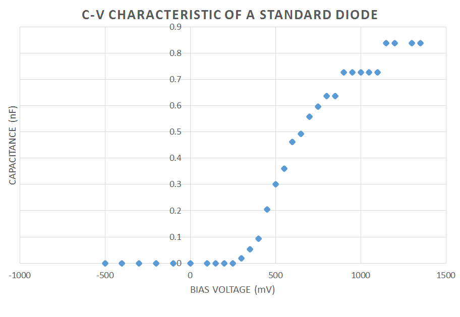
The standard diode will have a small amount of capacitance current flows across it. This capacitance is called the Junction Capacitance and is because charge is stored inside the diode and a small amount will build up. Figure 2 is C-V characteristic of the P6KE6.8A diode, of which this is the spec sheet: P6KE_spec_sheet. This data was taken using a voltage divider, shown in Figure 3 and the voltage divider equation, . We also choose f=10 Hz, Vin=20 mV (AC Voltage peak to peak), R=1 kohm, and bias Voltage=-500 mV to 1200 mV). As you can see, when reverse biased the voltage was basically zero, this is because the electrons and holes drift in the opposite direction and leave their respective n or p type region.
Carrier Dynamics
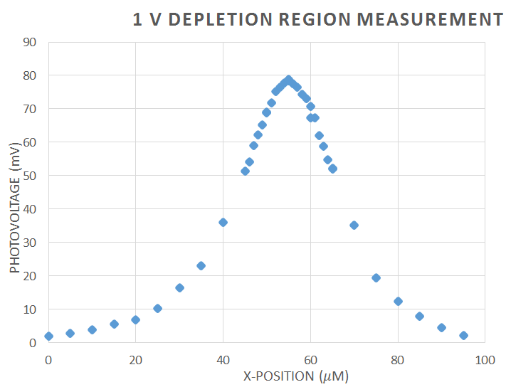
The setup shown in Figure 4 was used to measure the carrier dynamics of a laser diode. For this experiment, the GH0781JA2C was used, the spec sheet can be found here, GH0781JA2C_spec_sheet. We used the two lenses to expand and collimate the lens. This is important, because the microscope objective, which is focusing our beam down to a point in order to shine on the semiconductor of laser diode, is designed to be fully filled of light in order to work properly. The chopper was used to chop the light into a frequency in which other parts of the room where not emitting radiation at. This frequency was then sent to the lock-in amplifier, which amplifies the signal that goes in which is at only this frequency. This helps separate our data, the voltage over the laser diode, from the noise in the rest of the room. Before using the lock-in amplifier, we experienced trouble getting readings on the multimeter, which was measuring unchopped light. To fix this, we connected our diode with a coaxial cable instead of just plain wires. This was to protect the wires, which were acting as antennas and were picking up frequencies from other electrons in the room, so the lights, refrigerators, etc. This did fix the problem, but we still received significant noise, and thus used the lock-in amplifier. We used the 7280 whose instruction Manuel can be found here: 7280_spec_sheet_and_instruction_manuel The laser diode was also reverse biased. This is because there would be no voltage or current across the laser diode, and therefore the only voltage we would read would be that from focusing our IR diode laser (The _______) at 784 nm on the laser diode. The purpose was to measure the depletion zone of the diode, which we measured at -1 V, 0 V, and 1 V. The data is shown in Figures 5, 6, and 7 and is what we expected. The depletion region increases the more negative the bias across the diode. This is because the carries, electrons and holes, are evacuating the junction at negative bias, and thus the region with no carriers becomes larger. (Talk about beam width).
With the same setup we took band edge measurements. (Insert Theory) This was done by varying the wavelength of the tunable IR laser used in the carrier dynamics setup and directing the beam straight at the center of laser diode. The data found was conflicting and as seen in Figure 8, it varied a bit and flat lined at certian wavelengths. To fix this we added in a isolator and a wave plate that adjusted the polarity of our beam to that which the isolotor would allow to pass through. This was to remove any back reflection that may have been skewing our data. This did not fix the problem, so we took a spectrum of our laser at each wavelength, varying from 784 to 804 nm. As seen in Figure 9, the laser we were using does not tune past Figure 6 and at one point emits two wavelengths when it should be emitting one. For future band edge measurements, a different laser will have to be used.


