Cutting the Board
If the board is not roughly the shape of your lithographic film PCB then you'll need to cut the board. The fiberglass layer of a PCB can be extremely hard on tools and create dangerous silica dust when cut, thus cutting the board requires strong tools, a dusk mask and good ventilation. There are several ways to cut the board but using a diamond blade saw yields the cleanest cut with the most precision. Using a hacksaw is another method but the cuts will not be as straight and ventilation will not be ideal if this is done in the APL. It is also possible to cut PCBs with paper shear but this results in warped edges that will prevent your board from lying flat in the UV chamber (which is essential for the image transfer process from the lithographic film).
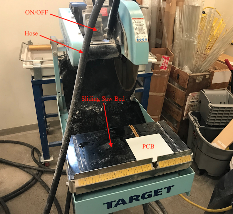
This makes using a diamond blade saw your best option. While there is a small diamond blade saw in the APL, I strongly recommend using the one in the craft center's Glass Shop (which is free for students to use). The glass shop is very well ventilated (make sure the fume hood in the room is turned on) and the saw blade has a source of running water that flows over the blade as it cuts, this is ideal for cutting glass/fiberglass because the water traps silica dust during the cut. Lastly, the saw in the craft center has a sliding bed for you to rest your PCB on, which will ensure a straight cut. Below is a labeled picture of the diamond blade saw I recommend you use:
Before you go to the craft center make sure you protect the board from sunlight on your way. For new boards the metallic bag the board comes in is sufficient, for older boards make sure you put the board in a UV blocking container when you go outside.
For those who haven't used the glass shop in the craft center, when you arrive tell the person at the front desk you would like to use the glass shop for "cold working" (this means you will not be using the glass furnace, which costs money), they may ask you to sign up for a term pass but this will be free for students. Next, ask for a pair of safety glasses and to talk to the glass tech on duty, this person will help you operate the saw if you've never used it before.
Now, if your PCB is new take your PCB out of the metallic bag. The PCB will have two layers of thin white plastic adhered to both sides, this is to protect the photoresist from UV light and scratches. Do not remove this layer until you are ready to expose the board in the UV curing chamber. Next, mark your PCB with a straight edge and maker to indicate your cut lines and then make your way to the saw. Although the glass tech should make sure the water is running over the saw blade before you make your cut, this step can be forgotten, so be sure to double check that water is dripping off of the saw blade before you use it. Cut your PCB and head back to the APL with the boards protected from UV light. Lastly, you'll want to carefully turn down down any cut edges. The copper will likely be bent along the edges from cutting the board so you must use a file to make these edges smooth. Your board is properly filed when both sides lay flat against a flat surface. Flat boards are necessary to ensure that the lithographic film lies flat on the board, if the film does not the image will lost resolution and make the the image on the board fuzzy.
