How to Make a Printed Circuit Board (PCB)
Contents
Using KiCAD
Youtube Tutorial
An in depth series of 10 youtube videos demonstrating the a KiCad project form start to finish.
Installing and Opening KiCad
The first steps in using KiCad.
Eeschema
Eeschema is the first program you'll use, where you'll create a digital copy of your circuit diagram and assign footprints to the different components. This will allow you to generate a netlist, which will be read into Pcbnew.
Footprint Editor
The Footprint Editor program may or may not be necessary but it allows you to draw new footprints or edit preexisting footprints. Footprints are necessary for every different component of your circuit, so the footprint editor becomes necessary if the footprint for your component is not already in one of the KiCad footprint libraries.
Pcbnew
Pcbnew is the program used after Eeschema. Pcbnew allows you to design the physical layout of your PCB and draw the copper connections between the your different components. All the information about the different connections and components is saved in the netlist so be sure to complete and upload your netlist before you begin.
Using gEDA
Tutorial from the program creators can be found here. [1]
Open the program gEDA Schematic Editor. (gschem)
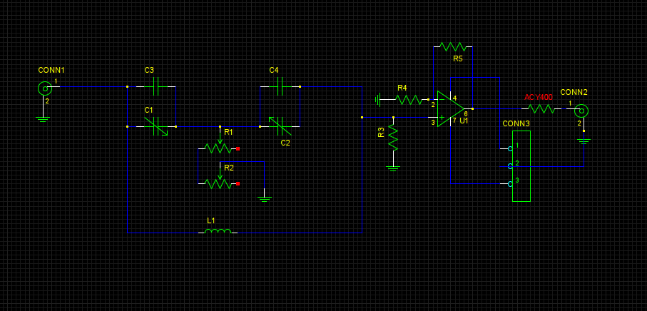
Choose Components and Build the Circuit
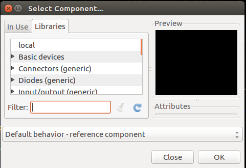
Using the Add component menu (looks like a 2 pronged power cable) select the various electronic components that will be on your board.
The filter option in this menu allows you to quickly type the part in order to find it rather than searching through the menus. (ie. ground or resistor)
Move the parts around similar to how they will be constructed on the board. This wont be the final layout, but make sure all necessary connections can be made. Then connect components by clicking the blue add nets mode button next to the add components button.
To de-select a component or a wire right click the mouse.
If you need to rotate or flip components for any reason, click on the component and then press er to rotate or ei to flip.
You can change the name and what is visible about the component by double clicking on it and changing the visibility settings and its attributes.
After the circuit is constructed and all connections are made correctly its time to add footprints to the components.
Assign Footprints
Footprints provide the information about the physical specifications of each part in the circuit such as size, number of pins, pin size... ect.
Most common circuit parts (resistors, caps,...) have pre-made footprints available, speciality parts need to have their footprints designed and saved. Once a footprint is made and saved it can be used in the future.
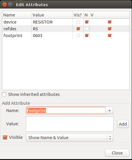
To assign a footprint to a commonly used part, double click on the component. Towards the bottom of the menu, below add attribute, select the name drop down menu. When the menu drops down, select footprint. In the value box, this is where you'll enter the code for the specific footprint needed. Common codes and naming conventions can be found at this website, [2]
After the value is entered, click add. Again keep in mind you can choose to make this footprint name not visible on the diagram. To assign the same footprint to multiple components, click on another component before closing the edit attributes menu, and again click add. This will add the previously chosen footprint to the newly selected component.
Custom Footprints
To build a custom footprint open the program pcb designer. The Via button in the lower left portion of the side bar menu corresponds to pins. Click and drag these vias where physical pins will. This requires measuring and planning on the physical component. There is mil measurements in the top right corner to tell where the cursor is so that you can be precise about where the vias are placed. Now you can highlight the entire footprint and then press (control x) this cuts the design to buffer. Then under the buffer menu, click convert buffer to element. This will place this element on the screen. Now, click and copy that element, and under the buffer menu, click save buffer to file. Save into a directory that can be accessed by gschem. In gschem for the footprint id, use whatever file name you save the custom footprint as.
Transferring to PCB Designer
When all components have a footprint and when all needed connections are made you are ready to send this blueprint to the pcb designer program. Save your file at this time(in the same directory that the custom footprints are saved to). Now in the command line use the command gsch2pcb. Make sure you are in the directory where the .sch file is. For example this is what your command line should resemble with different file names and in a directory where your file is saved. (gsch2pcb -d ~/pcb-mylib/ BridedTeePCB_preamp.sch).
When done successfully, the command line will give directions to continue. I have listed them below.
1. Run pcb on your file ie. BridedTeePCB_preamp.pcb
2. From within PCB, select File -> Load layout data to paste buffer and select BridedTeePCB_preamp.new.pcb (this will be you files name) to load the new footprints into your existing layout.
3. From within PCB, select File -> Load netlist file and select BridedTeePCB_preamp.net to load the updated netlist.
4. From within PCB, enter :ExecuteFile(BridedTeePCB_preamp.cmd) to update the pin names of all footprints.
PCB Designer
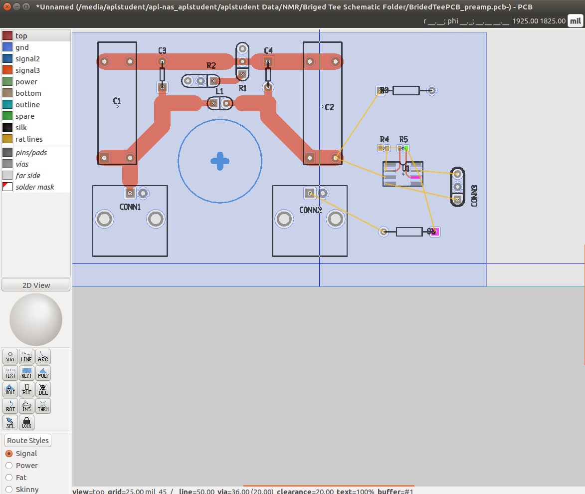
The last exercise should have transferred the information about all the needed components and connections to the PCB program. In this PCB program you will move the components by dragging and dropping them to where they will physically go on the board. The yellow rat lines connecting components show the needed connections. When you move multiple components press the o button to optimize and re-position the rats nest. Clicking on the ROT button in the bottom left menu bar allows you to click on components to rotate them. Once all components are placed where they are physically going to be on the board (allowing for the needed connections to be made) you are ready to begin drawing the copper lines. Note, if rat lines intersect that is okay, they simply show where connections need to be made. However when laying out components be aware that copper drawn in lines should not intersect unless they are meant to.
To begin drawing in copper lines first click on route styles in the bottom left corner. From there you can change the line width to you desired amount. (127 mm gives a characteristic impedance of 50 ohms). After this is selected you can zoom in and our using the mouse wheel hovering the mouse over where you would like to zoom. This is helpful where trying to see exactly where copper lines are being drawn. Next click on one of the signal tabs in the top left corner. it should highlight grey. Then click LINE in the bottom of this menu. Click to start drawing, each time clicking to change directions. When done drawing hit escape. Name another tab with GND and click on it so that it turns grey. Then with the RECT button in the bottom left, cover the entire board with a ground plane if one is needed. Then to connect components to ground, click on the THRM button in the bottom left and click the pins that will be grounded.
Printing the Transparency
After you are satisfied with the circuit make sure to save it and then go to file---> export and choose export to postscript. This provides a nice way to view each layer of the circuit before printing. Check the parody of the circuit layers in the exported postscript. If they need to be changed you can go back into the pcb program and after exporting to postscript, check the mirror option. Note, for print out transparencies you almost always want mirror selected, this is because the transparency is flipped and laid over the pcb before developing. Once you are satisfied with the post script diagrams open gimp photo editor and in gimp open the needed pages of the postscript (pgs 2 and 3 are the top and bottom). Import at 600 dpi (resolution). Print a transparency of this on a high resolution printer.
Making the Board
Cutting the Board
Measure the dimensions of the printed transparency, and mark these off on the physical undeveloped PCB. With a heavy duty cardstock cutter line up the PCB such that the usable portion hangs to the left of the blade. This will minimize splintering of the board when it is being cut. When ready to cut, slice the board with force in one continuous motion. With a cut PCB, slightly larger than the transparency, you are now ready to develop the board.
Developing the Board
Exposure times for the PCB vary depending on the exposure method. For instance, if you're working with a single sided board and plan to develop using the overhead florescent lights I recommend about 15 minutes of exposure. Before peeling off the tape and exposing the PCB, make sure to have a flat plate of glass such that you can lay the transparency over the peeled board and then lay the glass over the transparency so that it is flat against the PCB. It is helpful to dim the lights during this step to minimize exposure until ready. Once exposure begins do not move the board.
If you are building a double sided board, it will be a good idea to use a uva light chamber so that you can expose evenly on both sides. If you do not have one here is a link to construct one using leds. [3] Another method to expose a double sided board without a light chamber is to secure the transparency on both sides of the board and then expose each side individually for the same amount of time.
Expose long enough such that all of the uncovered copper goes away but not so much such that the protected copper goes away. Note exposure times in a UVA chamber will be much less than 15 mins.
Once the board is necessarily exposed, develop the board by swishing the board around in a solution of NaOH. This should be done until the exposed portions (where light was able to hit the board) are clean copper. There should still be traces where the copper will be on the final product.
Etching the PCB
After the PCB has been developed wash it in a bath of copper chloride with a eye dropper worth of hydrochloric acid. Making sure to continuously swish the board around in order for the reaction to take effect. Wear gloves for this process. Continue until all of the unwanted copper washes away. All that should be left is the copper protected by the traces that were cured on from the transparency. Neutralize the board with a base to stop the reaction. When Finished, rinse the board in acetone to get rid of the trace ink. All that should be left on the board now is the wanted copper traces. Wash board in water and dry off after.
Populating the PCB
Before components can be soldered into the board, the necessary holes need to be drilled. The PCB program should have included where these holes need to be, or if you made a custom footprint you designed them with the via button. Place the PCB in a drill press. The chosen drill bit should be slightly larger than the components pin hole such that it can be soldered in. For most common electronic components use a #60 carbide drill bit. Make sure the drill bit is carbide tipped so that in doesn't break when cutting through the fibreglass PCB. Also make sure to wear goggles for this process as there will be fibreglass shards. Drill out necessary holes. Keep the fibreglass shavings in a pile and after drilling is complete, vacuum them up. The electronic components are now ready to be soldered in.


