Digital-Electronics Obstacle Course
Contents
- 1 Permanent Materials (located in the electronics area):
- 1.1 Materials to borrow when necessary
- 1.2 Activities
Permanent Materials (located in the electronics area):
- power supplies
- function generators
- oscilloscopes
- Fluke 179 multimeter (MM)
- capacitance meter
- electronic proto-boards
- wire, resistors, capacitors, inductors, diodes, Op-Amps, other ICs
Materials to borrow when necessary
- LTSpice circuit simulation software (on computers in lab)
- lab copy of The Art of Electronics, Horowitz & Hill (H&H)
- inductance meter
- Keithley voltage supply
Activities
- Read chapter 8 of Horowitz & Hill's The Art of Electronics.
- Read Chapters 10 and 11 of Keith Brindley's eBook Starting Electronics.
The Inverter or NOT Gate
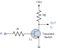
- Using T1 = TIP31C, R = 10k, R2 = 1k, Vcc = 10VDC construct the circuit shown at the right.
- Apply 0V to input A. What's the output Q?
- Apply 10V to input A. What's the output Q?
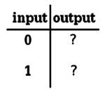
- Taking 0 (or close to zero) volts to be logic state "0" and 10 (or close to ten) volts to be logic state "1" construct the logic state truth table for this circuit (see right).
- What type of logic gate does the truth table indicate?
- Letting the input = A and the output = B write a Boolean statement describing this NOT gate (i.e., Q = ???).
We can also use the "True" and "False" representation of digital logic with a "0" state equated with a "False" value and "1" state equated with a "True" value. Yet another digital logic representation is the "High" and "Low" representation equated with the "1" and "0" states respectively.
The OR Gate
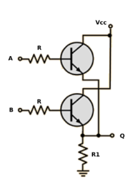
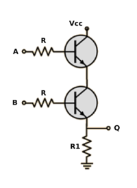
- Using two 2N4401BU transistors with R = 10k, R1 = 4.7k and Vcc = 6VDC construct the circuit shown at the right.
- Apply 0V to A and 0V to B. What is Q?
- Apply 1V to A and 0V to B. What is Q?
- Apply 0V to A and 1V to B. What is Q?
- Apply 1V to A and 1V to B. What is Q?
- Construct a truth table for this circuit.
- What type of logic gate does the truth table indicate?
- Letting the input = A and the output = B write a Boolean statement describing this OR gate.
The AND Gate
- Using two 2N4401BU transistors with R = 10k, R1 = 4.7k and Vcc = 6VDC construct the circuit shown at the right.
- Apply 0V to A and 0V to B. What is Q?
- Apply 1V to A and 0V to B. What is Q?
- Apply 0V to A and 1V to B. What is Q?
- Apply 1V to A and 1V to B. What is Q?
- Construct a truth table for this circuit.
- What type of logic gate does the truth table indicate?
- Letting the input = A and the output = B write a Boolean statement describing this AND gate.
The NOR, NAND, XOR and XNOR Gates
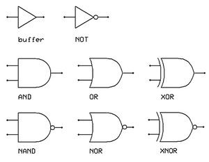
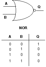
It should be clear that we could follow the OR gate with a NOT gate and get a NOT OR gate (a NOR gate).
We could follow an AND gate with a NOT gate and get a NOT AND gate (a NAND gate).
In addition, there are other basic gates like the XOR (exclusive OR) and the XNOR (exclusive NOR).
An OR gate outputs "True" when either (or both) of its inputs is "True". However, an XOR gate outputs True (we'll drop the quotes) when either of its inputs is True (but not both). The XNOR gate is a combination of an XOR gate and an inverter (a NOT XOR gate).
Digital ICs
It would be extremely tedious (though in principle possible) to build every logic circuit from discrete transistor elements. There are dedicated digital ICs that perform these logic functions reducing cost, saving time and generally making it easier to build complex digital circuits.
- The 7400 series digital ICs. These are robust TTL (transistor-transistor logic) devices and operate at 5V.
- The 4000 series digital ICs. These are (slightly less robust) CMOS devices and operate over a range of voltages.
Bistable Circuits - Flip-Flops - Digital Memory
The type of logic gates examined above are known as combinational (or time independent) logic gates. That is, their output is a function (only) of their present combined inputs. This means that combinational logic has no memory.
For a circuit to have memory its output must depend not only on its present input but also on its past input. Logic of this type is known as sequential logic. Virtually all circuits in practical digital devices are a mixture of combinational and sequential logic.
The SR-Type NOR Bistable or Latch
Recall that the NOR gate is an inverting OR gate. Also recall that an OR gate's output is High when either or both of its inputs is High. So, a NOR gate's output is High when both its inputs are Low and its output is Low for all else.
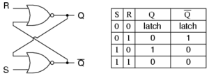
Now consider the NOR latch symbolic circuit shown at the right with both S and R initially Low (S and R stand for Set and Reset respectively). If S then goes High the output of S-gate is Low. And since the output of the S-gate is cross-coupled to the input of the R-gate the R-gate is High. This High from the R-gate output is then fed back into the S-gate input keeping the S-gate output low.
Now consider what happens when S subsequently goes Low. Since the input to the S-gate is now still a combination of a Low and a High its output is still Low. That is, the output is "latched" Low and Q is "latched" High regardless of subsequent changes in S. The outputs "remember" their states. The analysis remains valid when R and S are switched.
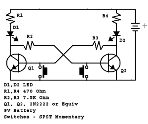
- Using a proto-board, two 2N4401BU transistors and LEDs build the flip-flop circuit shown at the right.
The outputs are the collector voltages and the inputs (S and R) are the switches. When the switches are set such that their bases and emitters are shorted R and S are both Low.
- Verify the S-R NOR latch function table.
In addition to the SR NOR bistable there is a SR NAND bistable. Beyond these there are other bistables with added functionality like the clocked SR bistable which allows several bistables to be synchronized. Like with the transistor logic gates considered above there are commercially available Latch ICs that are inexpensive and easy to use.
Timing
The Astable Multivibrator
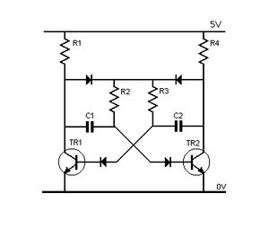
A circuit that is similar to the previous SR-type NOR latch is the astable multivibrator. Unlike the latch which is bistable (stable in either of two states) the astable multivibrator is not stable in either of two states. As such, it oscillates between the two states.
- Construct the circuit shown at the right using R1 = R4 = 5k, R2 = R3 = 1k and C1 = C2 = 1uF.
- What is the waveform?
- What is the waveform's frequency?
- Change C1 to 10uF. Has anything changed?
The 555 Timer IC
We've seen in the previous section that in principle it's possible to construct timing circuits with discrete transistors. However, as was previously the case concerning logic gates, this is a tedious task and there are a number of commercially available IC options. The 555 is a well known and used timing IC. It can function as a one-shot pulse generator, an oscillator or as a bistable flip-flop.
- Employ an LM555 and additional components to construct a free-running oscillator at around 500Hz with a duty cycle around 10%.
- Configure the LM555 for a one-shot pulse of width around 10ms.
Analog to Digital Conversion (ADCs)
- Read section 9.15-9.21 of Horowitz and Hill's The Art of Electronics.
How do we get continuous (analog) data into a digital computer? The answer is analog-to-digital conversion
Construct the circuit shown at the right. As Vin rises above Vn1/2/3/4 the output of OA1/2/3/4 goes high lighting up Led1/2/3/4.
The continuous, analog Vin is mapped to a discrete set of four output values.
- For Vin in the range of 0 to 12V (in 20 evenly spaced steps) plot the output voltage as a function of input voltage.
- Repeat the measurement but divide Vin's range into 5 and 10 steps. What changes?
- How would the output change if the input range was divided into 100 steps?
As was the case previously, there are a number of commercial ADCs that reduce cost and save time (see H&H Table 9.5).

