Preparing the UV Chamber and Board
Before getting any boards out, the UV chamber must be prepared. Get a VIS optical power meter (this detects light in the visible wavelength spectrum) out and lay the detector face down on the middle glass plate. Set the wavelength to 400nm (the actual wavelength is centered on 365; This introduces a roughly 40-50% shortage in measured power, if one is interested in absolute terms).
Plug the lid power connections in, turn the power level all the way off, close the lid and zero the OPM, and turn the chamber on. Dial the potentiometer until the power level reads about 200uW. Kill the power, remove the lid and put the OPM away.
Contents
Single Side Board
Exposure of a single side board is simple: Lay down bottom glass plate, peel the white protective coating off the circuit board and lay it sensitive side up (for a top-copper-only, presumably for an all-surface-mount circuit) or down (bottom-copper-only, typical of an all-through-hole circuit). Lay the film with emulsion in contact with the green photoresist, then lay the upper glass plate on top to acheive close contact. Small bits of aluminum scrap make good weights.
Double Side Board
At this point you should have both sides of your artwork printed on lithographic film. Before you expose the PCB, it is essential that the two pieces of film are aligned on either side of the board as precisely as possible. To achieve maximum precision, it is recommended to use the L-shaped aluminum jig is in the UV curing chamber.
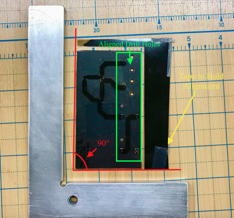
The first step is to cut one corner of your film artwork. Before you cut, line up both pieces of film as if you were to expose your board (that is, all the through holes match up) and tape the pieces of film together so that the drill holes stay aligned. Then, using a paper cutter to ensure straight cuts, make at least two cuts such that the edge of your artwork has a 90 degree corner. The edge of your PCB artwork should have edge cuts indicated which makes for an ideal way to align your corner cuts. Note: it is important that you cut both pieces of film simultaneously so that the the artwork stays aligned when the tape is removed. After the corner cut, make sure that the excess lithographic film is cut off.
The objective is to produce a corner in the artwork that fits into the jig while the artwork is aligned:
Now, remove the tape from the film and use the L shaped jig in the UV curing chamber to line up your bottom layer artwork, the PCB, and your top layer artwork. Lastly, place a sheet of glass on top of the artwork/PCB/artwork layer. The glass will keep all the different components lying flatly against each other.
It can be very difficult to lay the PCB on top of the bottom piece of lithographic film without moving the film, and also difficult to lay the top sheet of glass on top of the top piece of lithographic film without moving it. If you are having trouble with alignment you can see the alternative approach below or drill a few holes in the PCB to help you align the through holes or vias on the lithographic film.
An Alternative Alignment Approach:
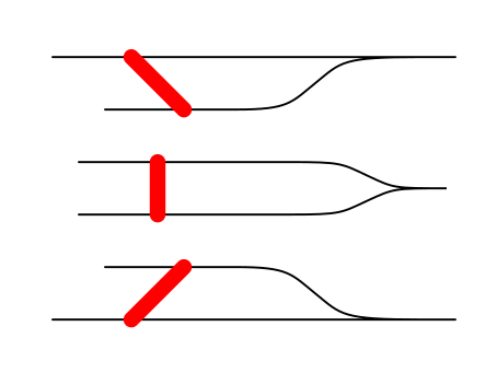
Making a double sided board introduces a new technical hurdle: The requirement that the near and far sides be aligned within a few thousands of an inch, with a completely opaque and finitely thick layer between them!
The finite thickness is very problematic as demonstrated above, because the parallactic shifts it can introduce (if the vertical placement of the two film joints is neglected) can easily be on the order of 50 mils, which is much, much larger than the top-bottom alignment tolerance (consider 5 mils an upper bound on acceptability).
A successful approach has been developed for lining up two-layer boards:
A 1/32" thick piece of steel is used. WIth two small bits double sided tape (DST), tack the bottom layer down to the steel, emulsion up. Lay a longer strip of DST across the top of this film, above where the plate is.
Now hold the light close and line the top film layer up on top of the bottom one. Through-hole pins provide convenient concentric circles to align on. Check for basic sanity - do the through-hole sets of pins associated with integrated circuits line up?
Making sure the films are still aligned - it is very difficult to not let them slip a few thousands of an inch - slowly bring the top layer film down and tape it to the bottom one. Now, *provided that the layers are not separated*, the images are vertically lined up.
Gently pluck the combined image off the plate and remove the DST used to hold it: The two pieces of film are now a unit.
When exposing, the double-side board goes between the films and the plate goes underneath the taped edge of the films. By doing this, the middle scenario in the posited alignment cartoon is (approximately) brought about because the plate, 1/32" thick, is half as thick as our prototype boards (1/16" thick). The thickness of the film (2.5 mil) and the tape (4mil) are uncompensated, but so it goes.
Once the film, plate and board are positioned, lay the upper thin glass plate down. Use some small aluminum blocks to provide a small amount of weigh-down; Upon very close inspection, it should be clear that there is no (or next to no) air gap between the emulsion and photoresist via lack of any shadow.
Exposure in the UV Chamber
Before you begin exposing your board, read the next section ([]) and make sure that you have a prepared tray of mixed NaOH and water nearby. The NaOH solution removes photoresist and you risk unintentional overexposure from over-head lighting if you leave your exposed board out while preparing the NaOH solution. Preforming the exposure step in the quantum optics room with only the green overhead lights on protects your board from the stray UV light of the florescent overhead lights.
With the board assembly on the middle glass plate, put the upper diffuser plate in place if appropriate, close the lid, and turn the chamber on. The eerie violet glow should immediately appear.
Minimum exposure time, with an Optical Power Meter (OPM) reading of 200uW, is roughly 1m30s. Because the lithographic film has an enormous contrast ratio, there is a substantial margin for overexposure.
The margin is NOT a thousand times one minute: Edge effects (light diffracting around borders, and arriving at an angle, etc) mean that excessive overexposure will cause sufficient exposure to strip the mask to gradually bleed outwards from intentionally-exposed areas.
Inadvertently, a board was exposed for 7 minutes; This was sufficient to cause isolated thin copper rings to shrink very appreciably.

