Difference between revisions of "Developing the Board"
Aplstudent (talk | contribs) |
Aplstudent (talk | contribs) |
||
| (9 intermediate revisions by the same user not shown) | |||
| Line 1: | Line 1: | ||
| − | + | To develop the board, you will need a room-temperature bath of NaOH and latex gloves (the NaOH is somewhat caustic and shouldn't make contact with your skin). The NaOH comes in granule form and must be mixed with room-temperature water (do not use hot water). Every, 10 grams NaOH must be mixed with 1 liter of water. Using an electronic scale, measure 5 grams of NaOH, and using a graduated cylinder measure 500 milliliters of water, then pour the contents into a plastic tray (the solution will react with metal so do not use a metal tray). Mix the NaOH/water solution thoroughly to ensure that you board develops evenly. | |
| − | + | Once the solution is well mixed, use a gloved hand to gently submerge your PCB (the layers of photo resist can be damaged if the PCB isn't handled with care). The photoresist on the board should begin to "smoke" off immediately and you should keep the board moving to ensure fresh NaOH covers the board. The pattern of your artwork should become visible as the board develops. | |
| − | + | Check your board every 30 seconds to see the progress; 3 minutes in the NaOH bath was found to be effective. When the copper layer is exposed and shiny you are almost done. Once it looks as if all the photoresist has been removed continue moving the board in the solution for 30 more seconds. Then, remove the board and run it under cold water and be sure to avoid dripping developer during the transfer process. | |
| − | + | To dry the board, gently DAB the surface using a paper towel. DO NOT rub the board; the resist isn't a delicate flower but it's not that tough either. | |
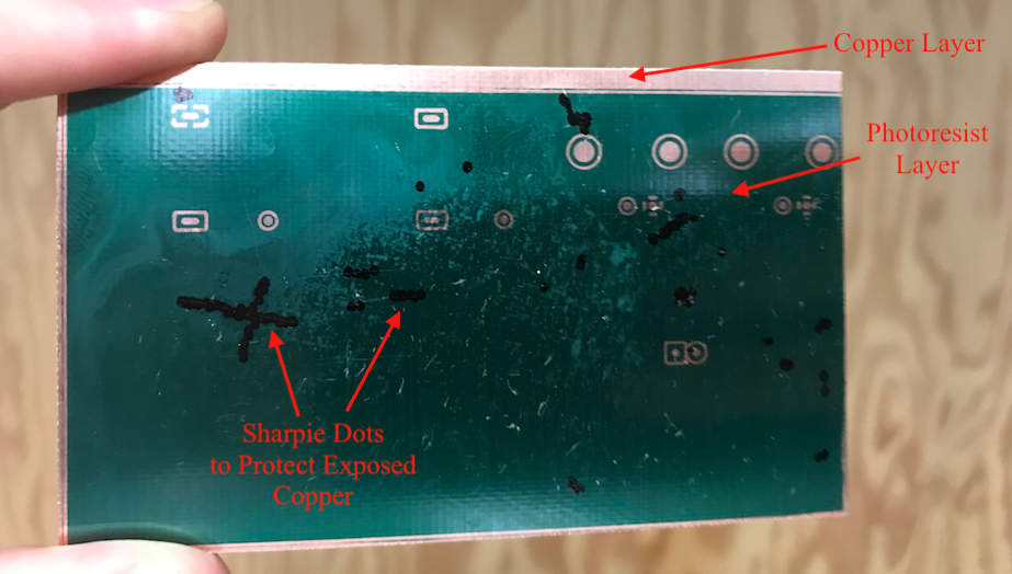
| − | + | After your board is developed you will have an exposed layer of copper, which will be etched away, and green traces of photoresist, which will protect the copper layer below. After developing, but before etching, the board will look like this: | |
| + | |||
| + | [[File:Developed PCB PM.png]] | ||
| + | |||
| + | |||
| + | Note: if any photo resist is accidentally scratched off you can make a series of dots with a sharpie, this process uses to ink help protect the copper layer during the etching process. This doesn't always work but it is better than leaving the copper completely exposed. | ||
| + | |||
| + | (Some of this tutorial is based on Professor Steck's tutorial in his book "Analog and Digital Electronics") | ||
Latest revision as of 12:43, 9 March 2019
To develop the board, you will need a room-temperature bath of NaOH and latex gloves (the NaOH is somewhat caustic and shouldn't make contact with your skin). The NaOH comes in granule form and must be mixed with room-temperature water (do not use hot water). Every, 10 grams NaOH must be mixed with 1 liter of water. Using an electronic scale, measure 5 grams of NaOH, and using a graduated cylinder measure 500 milliliters of water, then pour the contents into a plastic tray (the solution will react with metal so do not use a metal tray). Mix the NaOH/water solution thoroughly to ensure that you board develops evenly.
Once the solution is well mixed, use a gloved hand to gently submerge your PCB (the layers of photo resist can be damaged if the PCB isn't handled with care). The photoresist on the board should begin to "smoke" off immediately and you should keep the board moving to ensure fresh NaOH covers the board. The pattern of your artwork should become visible as the board develops.
Check your board every 30 seconds to see the progress; 3 minutes in the NaOH bath was found to be effective. When the copper layer is exposed and shiny you are almost done. Once it looks as if all the photoresist has been removed continue moving the board in the solution for 30 more seconds. Then, remove the board and run it under cold water and be sure to avoid dripping developer during the transfer process.
To dry the board, gently DAB the surface using a paper towel. DO NOT rub the board; the resist isn't a delicate flower but it's not that tough either.
After your board is developed you will have an exposed layer of copper, which will be etched away, and green traces of photoresist, which will protect the copper layer below. After developing, but before etching, the board will look like this:
Note: if any photo resist is accidentally scratched off you can make a series of dots with a sharpie, this process uses to ink help protect the copper layer during the etching process. This doesn't always work but it is better than leaving the copper completely exposed.
(Some of this tutorial is based on Professor Steck's tutorial in his book "Analog and Digital Electronics")
