Difference between revisions of "Pcbnew"
Aplstudent (talk | contribs) (→Generating Gerber Files) |
Aplstudent (talk | contribs) (→Generating Gerber Files) |
||
| Line 35: | Line 35: | ||
The "Plot" window should look something like this when you create your Gerber and drill files: | The "Plot" window should look something like this when you create your Gerber and drill files: | ||
| − | [[File:]] | + | [[File:KiCad_Pcbnew_Plot.png]] |
==Return to [[How to Make a Printed Circuit Board (PCB)]]== | ==Return to [[How to Make a Printed Circuit Board (PCB)]]== | ||
Revision as of 15:34, 4 February 2019
Pcbnew is where your'll design the physical layout of your board using the components and footprints from your netlist. To open Pcbnew return to startup KiCad window and select Tool -> Run Pcbnew. With the Pcbnew window open select File -> Page settings. This will bring up a menu that allows you to title and author your schematic. In the "Title" section write the title of your project and in the "Comment4" section write "Author: Your Name". Now you'll see your information saved in the bottom right of the red schematic page.
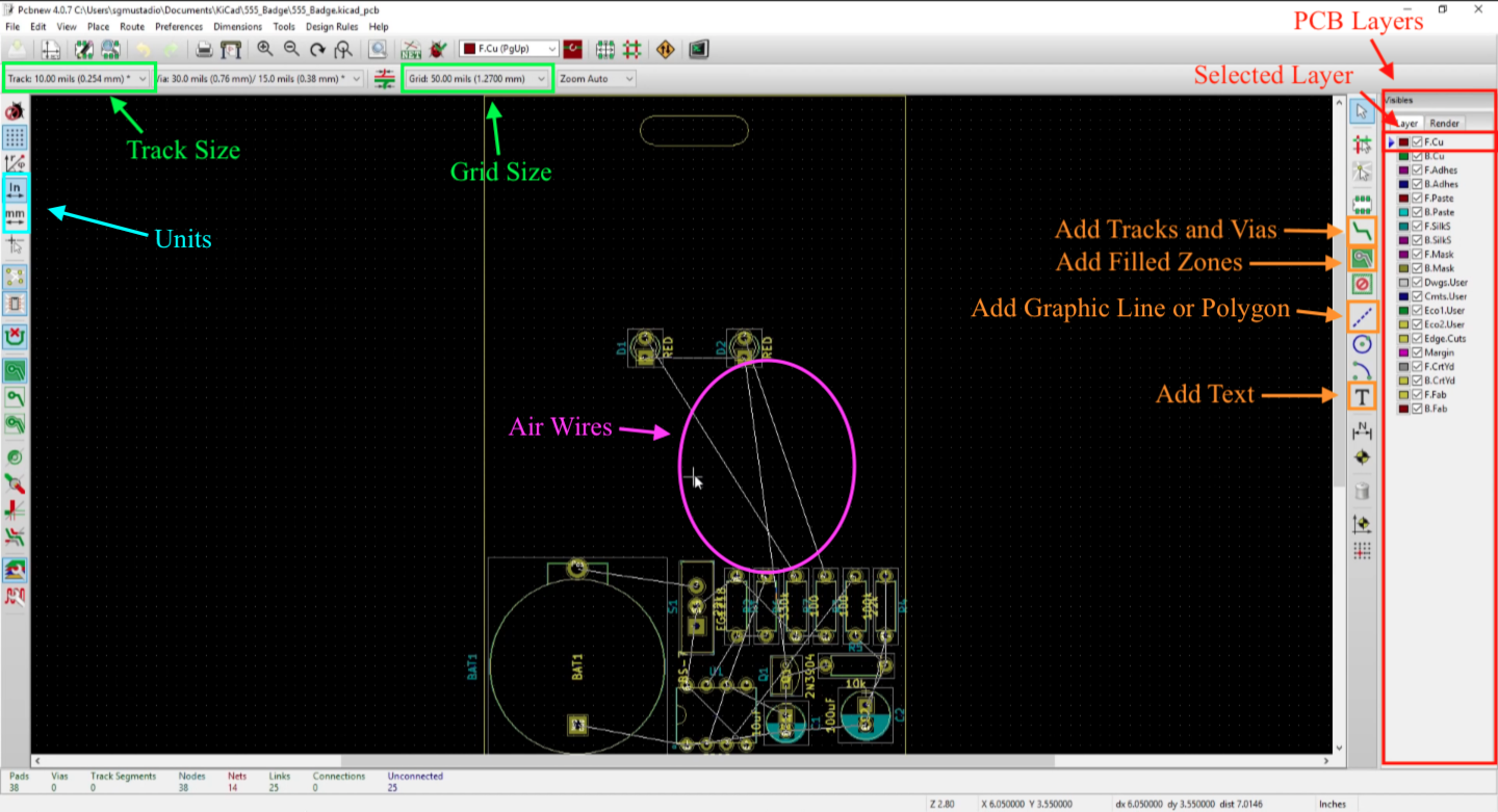
Below is a labeled screenshot of the Pcbnew window:
Contents
Importing Your Netlist
To import your netlist select Tools -> Netlist. In the popup window make sure that the "Netlist File:" shows a path to the .net file you just created. Now select "Read Current Netlist" and then click "Close". Now, all your components should appear in the center of the Pcbnew window. Now, you can press the "M" key to move the different components around. First you should just spread out the components so they are not overlapping. Next, you want to start arranging the parts according to how they will sit on your PCB. You'll notice the white lines (called air wires) extending between the different components, these are the connection lines and they make up what is called the rat's nest. You want to untangle this rat's nest such that no two air wires are overlapping, since overlapping copper tracks will short your circuit. If overlapping lines are unavoidable you'll need to create something called a via. This is a small hole in the PCB that will allow you draw a connection on the opposite side of the board. For a more detailed explanation of how to design your layout you can watch this video here. Lastly, you'll want to move all the components as close together as possible while making sure that the courtyards of the different components do not overlap. This will ensure that your PCB is as small as possible while still ensuring there is enough room for the different components.
Drawing Tracks
Once you've designed a board layout and moved your components to the appropriate places you can begin making the copper connections. To do this select Place -> Track and begin drawing the track from one pin to the next. You can tell which side of the board you are drawing your tracks on by looking at the layers column on the right. If F.Cu is selected then you will be drawing copper connections on the front of your board. If B.Cu is selected then you will be drawing on the back of your board. It is also important to make sure your track's width is appropriate for the amount of current flowing through it. Using this calculator you can calculate how much impedance your copper track will have and adjust your track width accordingly. If you're not sure about this try to talk to someone with PCB experience. To change the track width click Design Rules -> Design Rules, in the popup window you can adjust the track width column to suit your needs.
Indicating Edge Cuts
Indicating your edge cuts will help you see the size of the PCB and would be necessary if you were to send your schematic to a board house to be printed. The edge cuts indicate where the edge of your board will need to be cut. The area inside your edge cuts will be the size of your board. This means that if you need your board to be a specific size and shape you'll need to make sure the edge cuts reflect those needs. You can indicate your edge cuts by using the "Add graphic line or polygon" tool (the icon is in the right column of icons) and selecting the Edge.Cuts layer from the layers column. Draw the shape of the board around your components and make sure they all fit inside the space appropriately.
Adding Filled Zones
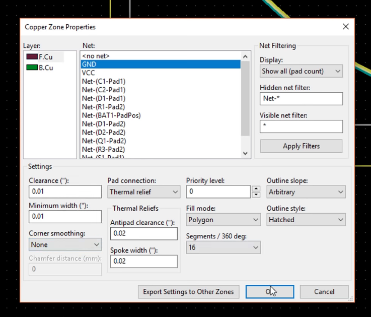
Filled zones are ideal for something like a ground plane. This means that a large area will be filled with copper and thus specific traces (tracks) will not need to be drawn. Often, the back of a PCB will the ground plane since many components are connected ground. To create a filled zone select the "Add filled zones" icon from the right column of icons. Now, left click anywhere on the schematic and you will be prompted with a "Copper Zone Properties" menu. Here you can specify which layer your filled zone will be applied to and to which net. To create the custom ground plane select the back layer, B.Cu, and select GND for the net. You can also adjust the clearance and minimum width, which will change how much space boarders your filled zone.
The "Copper Zone Properties" menu looks like this:
Generating Gerber Files
Once your board layout is complete (all components are connected by tracks or filled zones and edge cuts are indicated) you are ready to create Gerber and drill files. Gerber and drill files are a collection of files that isolate each layer of the PCB and contain the track and drill information for the layer. Gerber files are the PCB industry standard for formatting and are used to create the transparencies that are required in the developing step of PCB production.
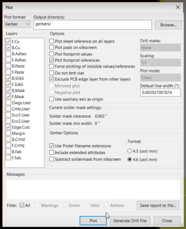
To generate Gerber and drill files select File -> Plot in Pcbnew. In the popup menu, next to "Output directory:" select "Browse..." and in your project directory click the "Create Folder" button in the top right corner. Name this new folder "Gerbers" and select it by clicking "Open". Now, in the layers section, make sure F.Cu, B.Cu, B.SilkS, F.SilkS, B.Mask, F.Mask, and Edge.Cuts are all selected. Now, click "Plot" to generate the Gerber files and select "Generate Drill Files" to make files with the drill hole information.
The "Plot" window should look something like this when you create your Gerber and drill files:


