File:Semi1.jpg

One goal of the Carrier Dynamics in a Semiconductor Device project is to measure captured carriers within the band-gap of a semiconductor. If a carrier (a hole or electron) is captured and then released in the band, the capture center is called a trap. These traps arise from defects or impurities in the material. One technique for measuring these traps is through Deep Level Transient Spectroscopy, or DLTS. This technique essentially measures the change in capacitance of the semiconductor.
A semiconductor is usually formed from two different types of materials, one which will be highly doped with holes i.e. p t-type(or an atom that can easily accept an electron) and doped with electrons i.e. n-type(atom that can easily give an electron). When these two materials make contact, there is an imbalance of charge that want to return to equilibrium. In doing so, some of the electrons from the n-type diffuse into the p-type, combing with some of the holes. The same goes for the other side. When this process stops, we have what is called a depletion layer, or potential barrier. This barrier represents the electric potential that is needed to overcome if any current is to get through. When reverse-biasing the semiconductor, the p side is made more negative from electrons flowing in, causing the potential barrier to increase. When it is forward biased, the p side becomes less negative, thus decreasing the potential barrier to the point where current can flow through.
During these forward and reverse-biased pulses, there will be a change in the electron occupation of a trap from the steady state value, Because capacitance is a measure of charge, a change in the electron occupation will create a change in the capacitance.
![{\displaystyle n1=[e2/e1+e2]N}](https://wikimedia.org/api/rest_v1/media/math/render/svg/bf38570612ac30677f075df94792b58226b01eb5)
Because the capacitance decays back to equilibrium quickly, we need a circuit that is capable of making measurements very fast. This can be done by using fast-recovery diodes, typically around 40 nanoseconds. We must place the diode sample in a two-legged circuit. The first leg will have the reverse-biased diode. The second leg will have a 180* transformer with an attenuation network. This will phase shift the incoming rf signal to where only a very small current will flow through. When a bias pulse from a generator is sent through, we will see a small change in the diodes impedance. This small impedance change will then create a small change in the rf signal, which can then be amplified and sent to a lock-in-amplifier for observation.

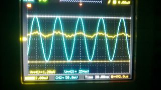
Here we see a recovery time on the order of 40 nanoseconds.

We have a power drop of nearly -130 db, essentially zero.
This technique requires the use of delicate equipment, which must be protected from any surges. This is achieved by using two sets of crossed diodesand a quarter-wave transmission line. The first set is placed between the pulse generator and the rf signal generator. This pair of crossed diodes acts as a high series impedance in between pulses, and shows a low impedance during pulses. This protects the rest of the circuit from any noise. Right before the amplifier, the signal will go through a quarter-wave transmission line. A quarter-wave transmitter is mainly used to match impedances, but here we will be using it to achieve infinite impedance. This is done because the transformer acts according to

Remember that diodes posses the property of having roughly a voltage drop of 0.6 volts. This means that we need at least this much voltage to get any significant amount of current through the diode. The quarter-wave transformer coupled with the shunt crossed diodes can now exhibit an infinite impedance. During pulses the current will go through the shunt diodes to ground, acting as a short. need another pair of crossed diodes, this time shunted to ground.
File history
Click on a date/time to view the file as it appeared at that time.
| Date/Time | Thumbnail | Dimensions | User | Comment | |
|---|---|---|---|---|---|
| current | 16:45, 13 December 2013 | | 1,632 × 918 (312 KB) | Wikiuser (talk | contribs) |
- You cannot overwrite this file.
File usage
The following page links to this file: