Carrier Dynamics in a Semiconductor Device
Physics of Semiconductors Wiki Page
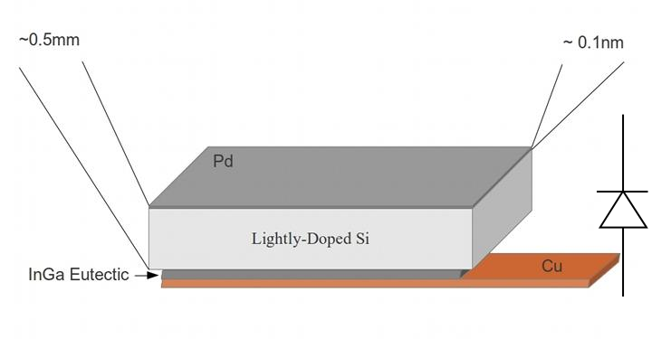
Schematic of Schottky diode semi-conductor
device pictured below-right.
Making Ohmic contacts
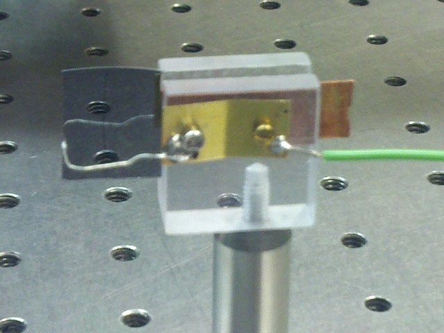
Schottky diode in mount with
electrical contacts: The actual diode
is an ~ 1mm diameter (unseen in photo) area on the silicon wafer
fragment. The 1mm diode is on the left edge of the wafer and is cut
in half so light can be introduced from the side and spatially scanned
across the junction area.
is an ~ 1mm diameter (unseen in photo) area on the silicon wafer
fragment. The 1mm diode is on the left edge of the wafer and is cut
in half so light can be introduced from the side and spatially scanned
across the junction area.
Other samples: 1cm diameter, 0.5nm gold layer on n-type, 650um thick Si wafer
face is [100], 1-10 Ohms-cm.
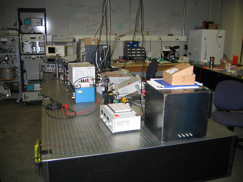
Our test setup.
Carrier-Dynamics-of-Semiconductors (pdf)
Links:
Schottky barrier - Wiki
Metal-Semiconductor Junctions - Pdf
Principles of Simiconductor Devices - Van Zeghbroeck